
Enabling memory redundancy during testing

a technology of memory redundancy and testing, applied in information storage, static storage, digital storage, etc., can solve the problems of affecting the manufacturing yield of these chips, the substantial cost associated with chip repair, and the repetitive and predictable design of these chips. achieve the effect of enabling redundant memory elements and avoiding the testing of unused redundant memory elements

Inactive Publication Date: 2005-12-08
MARVELL ASIA PTE LTD
View PDF7 Cites 18 Cited by
  • Summary
  • Abstract
  • Description
  • Claims
  • Application Information

AI Technical Summary

Benefits of technology

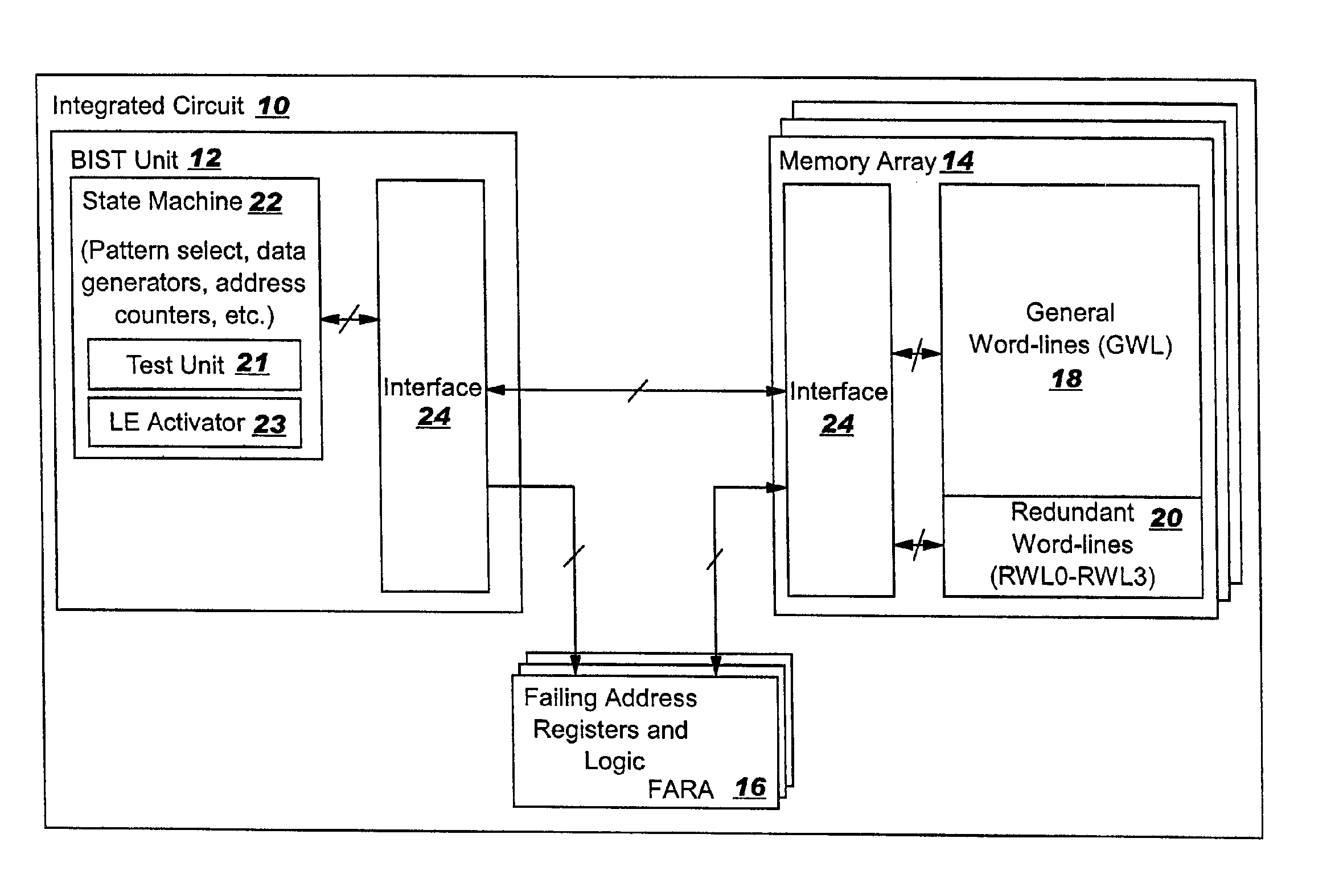
[0008] The invention relates to methods and apparatuses for enabling redundant memory elements during testing of a memory array. The invention provides testing of a redundant memory element only when the redundant memory element has been enabled to replace a failed memory element. Hence, testing of unused redundant memory elements is avoided. The invention implements a built-in self test (BIST) unit that runs multiple patterns while testing the memory to isolate and detect specific faults. The invention repairs any newly-found faults with redundant memory elements at multiple points during test such that faults are detected and repaired early without causing false failures. Faults in activated redundant memory elements are then tested in subsequent pattern tests. As a result, all faults in the general memory elements space will eventually be repaired through testing and repairing the redundant memory elements as they are enabled to make a repair. Since repair occurs during testing, a user can repair memory at any time, e.g., during start up of an IC, rather than just during manufacture. This functionality allows repair of reliability failures that occur long after manufacture is complete, hence, preventing IC return to the manufacturer. In addition, the invention includes registers that include control bits that allow use of the same latches for collecting failing addresses and implementing the redundancy to replace them.

Problems solved by technology

These memory arrays often hurt manufacturing yields on these chips because they are such a large percentage of the chip and they tend to push the limits of a technology's manufacturing process.
However, their very repetitive and predictable design lends itself well to methods of repairing the memories after the chip is manufactured.
This technique is favored because there is a substantial cost associated with repairing a chip.
However, this solution is inefficient and costly because defects found in redundant memory elements that are not needed to repair a chip will result in repairable chips being thrown away.
However, this technique does not identify failing redundant memory elements until after fuse-blow, thus incurring the added costs of test time, fuse-blow, and possibly packaging into a module (which often comprises half the cost of a chip or more).
However, additional costs of silicon chip area and test complexity are introduced.
This extra cost is justifiable in a high-density memory array such as a dynamic RAM (DRAM,) but is not acceptable for higher-performance, lower-density memories such as SRAMs and register arrays (RAs).
An additional cost is the extra test time incurred in testing the chip again at the same conditions after the memory elements have been replaced, as in the second technique.
Compilable (or customizable) memory presents further obstacles to implementing and testing redundant memory elements.
For instance, testing and mapping around failed redundant memory elements is much more cumbersome in a compilable memory design.

Method used


Image

  • Enabling memory redundancy during testing
  • Enabling memory redundancy during testing
  • Enabling memory redundancy during testing

Examples


case 1

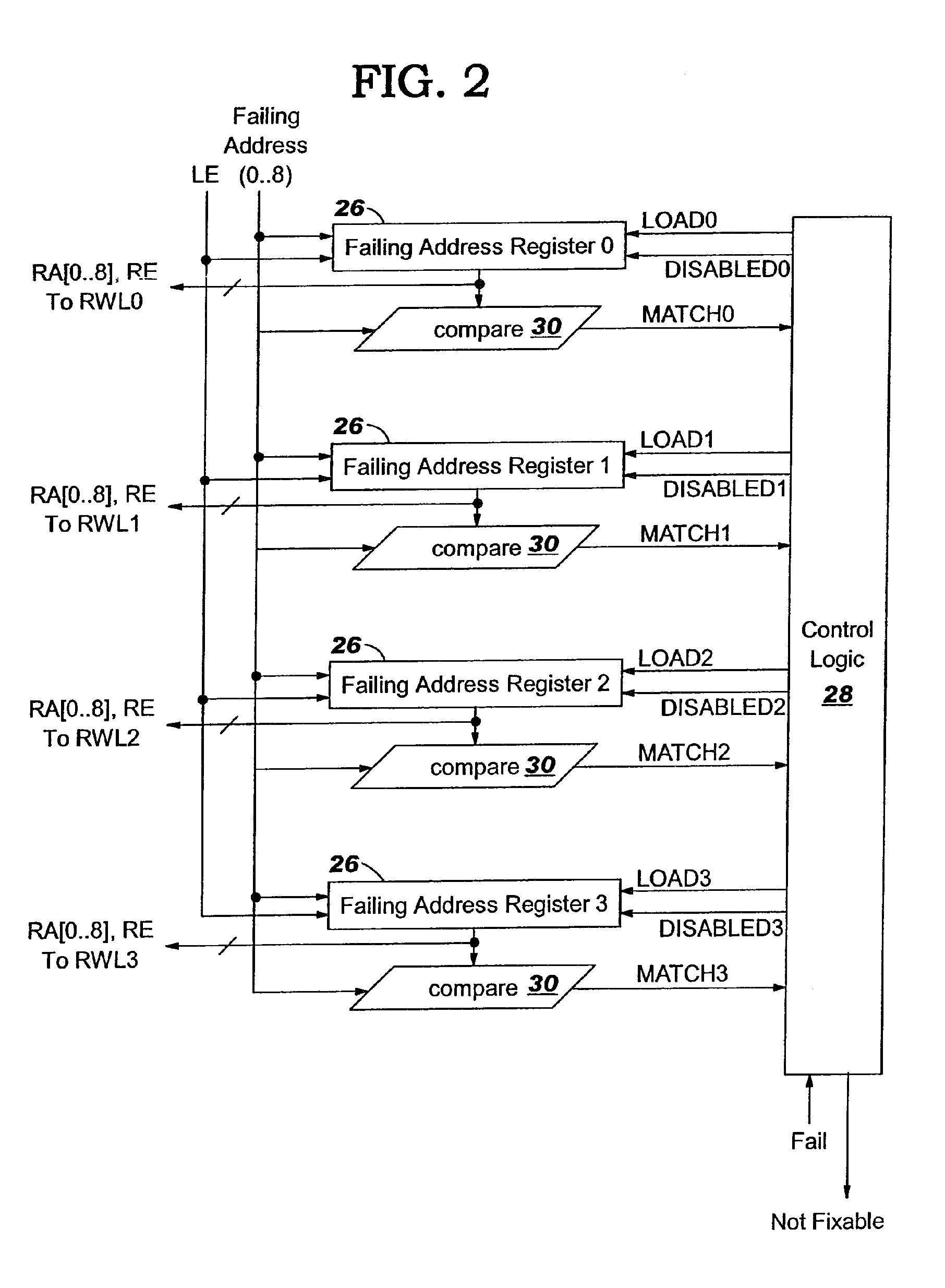
[0033] If the failing address does not match the contents of any FAR 26, then the failing address is loaded into the next available FAR, and the corresponding temporary enable bit TE bit of the next available FAR is set.

case 2

[0034] If the failing address matches at least one FAR address and both temporary-enable bit TE and enable bit EN for each matching FAR 26 are not set, then the failing address is loaded into the next available FAR, and the corresponding temporary-enable bit TE of the next available FAR is set.

case 3

[0035] If the failing address matches one FAR, and enable bit EN for this FAR 26 is set, and both the temporary bad-redundancy bit TB and bad-redundancy bit BR for each matching FAR are not set, then the failing address is loaded into the next available FAR, the corresponding temporary-enable bit TE of the next available FAR is set and temporary bad-redundancy bit TB for this matching FAR is set.

[0036] In all other cases, none of the FAR contents are updated.

[0037] At some point(s) during test, LE activator 23 activates load-enable signal LE which forces the value of temporary-enable bit TE to load into enable bit EN and resets temporary-enable bit TE. When enable bit EN is set to a “1” and bad-redundancy bit BR is not set “0,” AND gate 32 enables (via redundancy enable (RE) signal) the RWL in memory array 14 to replace this address, i.e., the redundant address (RA). Similarly, when LE activator 23 activates load-enable signal LE, it forces the value of temporary bad-redundancy bi...


PUM


Abstract

Methods and apparatuses for enabling a redundant memory element (20) during testing of a memory array (14).

Description

TECHNICAL FIELD [0001] The present invention relates generally to enablement of memory redundancy. BACKGROUND ART [0002] Memory arrays in general, and static random access memories (SRAM) specifically, account for most of the silicon area on many application specific integrated circuit (ASIC) chips. These memory arrays often hurt manufacturing yields on these chips because they are such a large percentage of the chip and they tend to push the limits of a technology's manufacturing process. However, their very repetitive and predictable design lends itself well to methods of repairing the memories after the chip is manufactured. The typical approach to memory repair is to include extra, or “redundant,” rows or columns which will be “swapped” with memory elements which have defects. Conventional methods for testing and repairing fixed-design SRAM memory arrays which include row, i.e., wordline, redundancy fall into three general categories. [0003] One technique stipulates testing all ...

Claims


Application Information

Patent Timeline
IPC IPC(8): G11C29/00G11C29/14G11C29/24G11C29/44
CPCG11C29/14G11C29/4401G11C29/44G11C29/24
Inventor OUELLETTE, MICHAEL R.ROWLAND, JEREMY
Owner MARVELL ASIA PTE LTD
Learn More