Liquid crystal display device

a liquid crystal display and display device technology, applied in the direction of optics, instruments, printed circuit aspects, etc., can solve the problems of large power consumption, large drive circuit, and longitudinal smear (crosstalk) that is produced in a direction along the drain line, and achieves low aperture efficiency, high aperture efficiency, and aperture efficiency over 50%

Inactive Publication Date: 2005-11-17
OHTA MASUYUKI +3
View PDF25 Cites 8 Cited by
  • Summary
  • Abstract
  • Description
  • Claims
  • Application Information

AI Technical Summary

Benefits of technology

[0015] Reference electrodes are formed on an organic insulating film in such a manner that the reference electrodes are completely overlapped on drain lines formed on one transparent substrate side in a plan view; and, hence, almost all of the unnecessary lines of electric force which are generated by the drain lines are terminated at the reference electrodes. Ac6ordingly, the crosstalk due to the leakage electric field which is peculiar to a display system, such as the display system of the present invention which adopts a transverse electric field, can be resolved. In this manner, the leakage electric field is more completely shielded than it would be by the shield electrodes which have been conventionally disposed at both sides of the drain line or on the counter substrate; and, hence, the horizontal direction of the pixels can be occupied by the display electrodes, reference electrodes and opening portions. Furthermore, it is also unnecessary to hide the gap between the drain line and the reference electrode, and, hence, a light insulating film (black matrix) in a vertical direction can be eliminated. Therefore, a low aperture efficiency, which is the largest defect in the display system adopting a transverse electric field, can be drastically improved and an aperture efficiency exceeding 50% can be realized. Namely, according to the present invention, a high aperture efficiency and a low smear condition are compatible. (Operation 2)
[0016] The specific dielectric constant of the organic insulating film is approximately half (the specific dielectric constant er being approximately 3) that of the inorganic insulating film. Furthermore, since the thickness of the organic passivation layer can be easily increased compared to the inorganic passivation layer, the distance between the drain line and the reference electrode is expanded. Even when these drain lines are entirely covered with the reference electrodes, the capacity formed between the drain lines and the reference electrodes can be made considerably small. Accordingly, the load as seen from the drain lines is reduced, so that the wiring propagation delay of the image signal becomes small, and the signal voltage is sufficiently charged into the display electrodes and the drive circuit for driving the drain lines can be minimized. <Operation 3>
[0017] The organic passivation layer has an excellent flatness so that when the organic passivation layer is coated on the uppermost layer of the substrate which constitutes an active element, the flatness of the substrate which constitutes the active element is enhanced. Accordingly, the irregularities of the brightness (transmission factor)-voltage characteristics caused by the irregularities of the gap between the substrates can be eliminated thus enhancing the uniformity of the brightness.

Problems solved by technology

However, a liquid crystal display element having the above-mentioned construction still has a problem in that an unnecessary electric field generated by the drain lines causes fluctuation of an electric field between the display electrodes and the reference electrodes, and so a bad image quality in which stripes are produced in a direction along the drain lines, or a so-called longitudinal smear (crosstalk), occurs.
The liquid crystal display element having the disclosed construction, however, is provided with shield electrodes and an electric potential is supplied from the outside; and, hence, it still has problems in that the charging or discharging of an electric current to a capacitance between the shield electrodes and the signal electrodes is large, the load on the drive circuit is large thus making the power consumption large and the drive circuit large, and a connecting means for applying the electric potential to the shield electrodes becomes necessary, thus increasing the steps and giving rise to connection failures.

Method used


Image

  • Liquid crystal display device
  • Liquid crystal display device
  • Liquid crystal display device

Examples


embodiment 1

>

[0044] Hereinafter, an embodiment where the present invention is applied to an active matrix system color liquid crystal display device will be explained. In the drawings, elements which have the same function are indicated by the same symbols and a repeated explanation thereof is omitted.

>

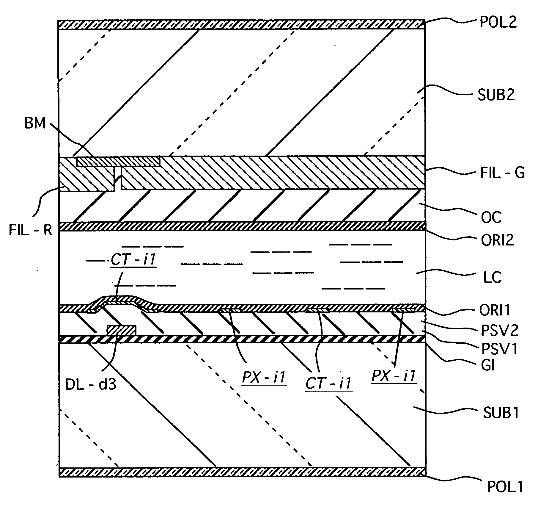
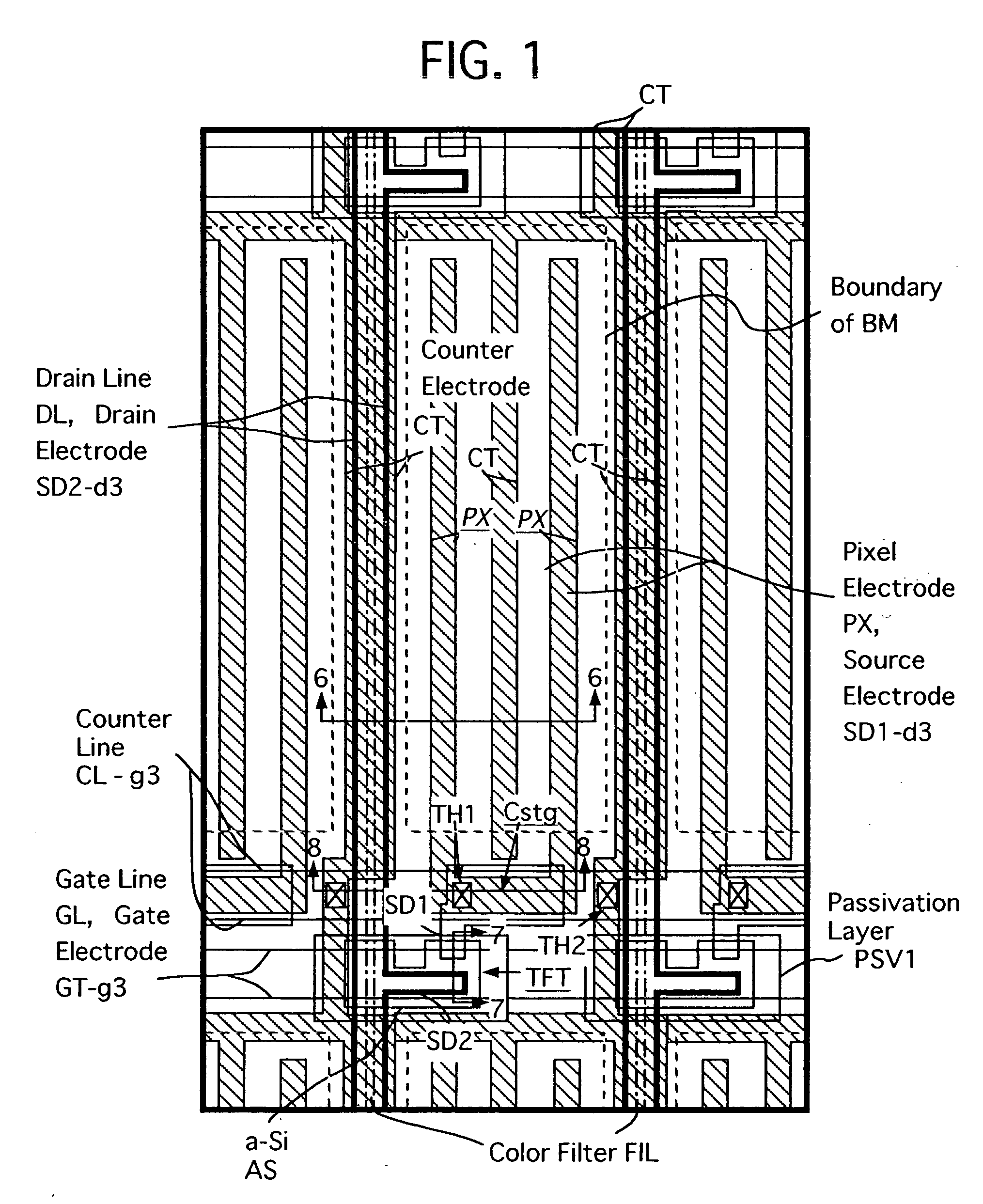
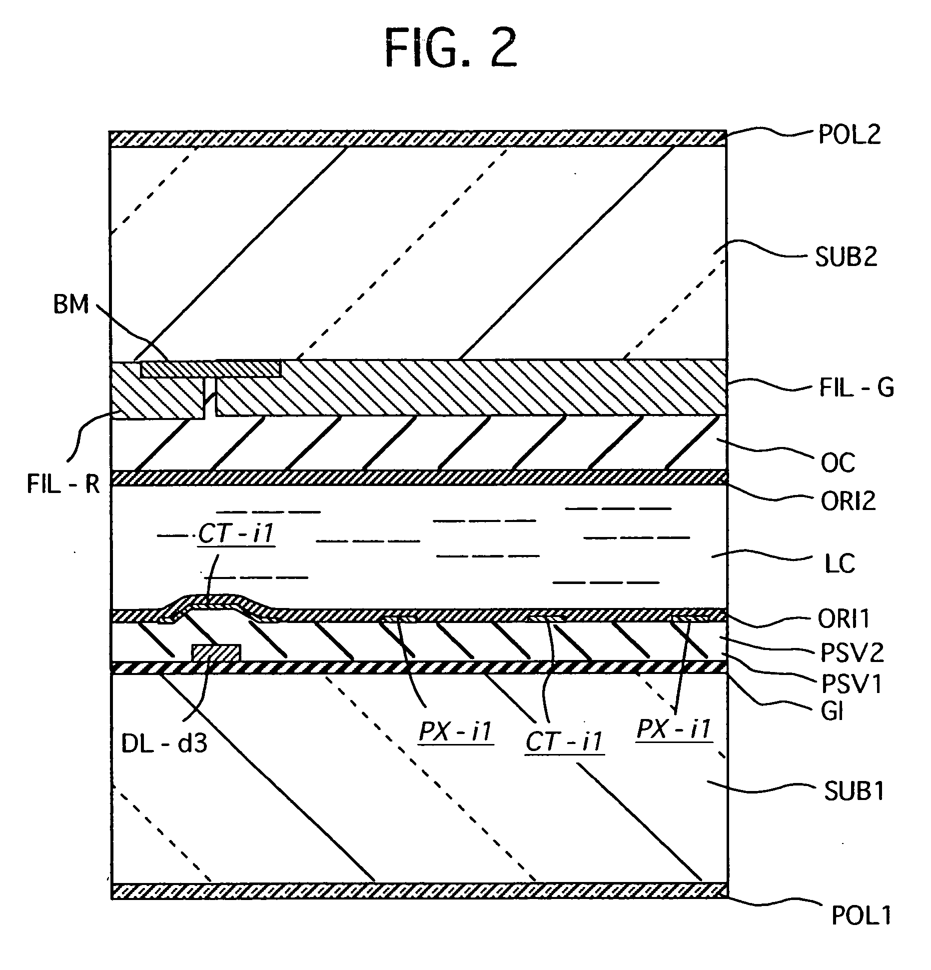
[0045]FIG. 1 is a plan view showing one pixel and its periphery of the active matrix system color liquid crystal display device of the present invention.

[0046] As shown in FIG. 1, each pixel is disposed in an intersect region (region enclosed by four signal lines) defined by a gate line (scanning signal line or a horizontal signal line) GL, a counter line (counter voltage signal line) CL, and two neighboring drain lines (image signal lines or vertical signal lines) DL. Each pixel includes a thin film transistor TFT, a storage capacitance Cstg, a pixel electrode PX (called a pixel electrode in this embodiment and acts as a display electrode) and a counter electrode CT (called a counter electrode...

embodiment 2

[0146] The present embodiment is the same as the embodiment 1 except for the following conditions. FIG. 20 is a plan view of the pixel and FIG. 21, is a cross-sectional view of a comb-shaped electrode portion.

>

[0147] In this embodiment, the pixel electrode PX is comprised of a source electrode SD1, a drain electrode SD2 and a conductive film d3 on the same layer as the drain electrode SD2. Furthermore, the pixel electrode PX is integrally formed with the source electrode SD1.

[0148] According to this embodiment, in addition to the effects of the first embodiment, a contact failure with the pixel electrode PX can be avoided, although the transmissivity is sacrificed. Furthermore, since the pixel electrode PX is covered with an insulating film (the passivation layer PSV1), when an orientation failure occurs, the possibility that a direct current will flow through the liquid crystal is lowered, thus eliminating a deterioration and the like of the liquid crystal, so that the reliabilit...

embodiment 3

[0149] The present embodiment is the same as the embodiment 1 except for the following conditions. FIG. 22 is a cross-sectional view of the pixel of this embodiment.

[0150]1, Organic Passivation Layer PSV2>>

[0151] In this embodiment, the passivation layer PSV1 and the organic passivation layer PSV2 are collectively removed, such that the external connecting terminals DTM, GTM are exposed. Accordingly, in contrast to the embodiment 1, the passivation layer PSV1 is formed on most of the pixel. Furthermore, in the pixel portion, for assuring an electric connection between the counter line CL and the counter electrode CT, which will be explained later, and an electric connection between the source electrode SD2 and the pixel electrode PX, through holes TH2 and TH1 are formed. At the through hole TH2, the organic passivation layer PSV2, the passivation layer PSV1 and the insulating film GI are collectively subjected to working and a hole which reaches the layer g3 is formed, while at the...


PUM

PropertyMeasurementUnit
specific dielectric constantaaaaaaaaaa
thicknessaaaaaaaaaa
thicknessaaaaaaaaaa

Abstract

A display device includes a first conductive layer formed on a substrate, an insulating layer formed on a portion of the first conductive layer and having a flat plane and an edge, and a second conductive layer continuously formed on the flat plane of the insulating layer, on the edge of the insulating layer, and on another portion of the first conductive layer. The edge of the insulating layer has a region so that an angle formed between the edge of the insulating layer and the first conductive layer is changed to be small at a side near to the first conductive layer.

Description

CROSS REFERENCE TO RELATED APPLICATION [0001] This is a continuation of U.S. application Ser. No. 10 / 838,241, filed May 5, 2004, which is a continuation of U.S. application Ser. No. 10 / 366,410, filed Feb. 14, 2003, which was copending with U.S. application Ser. No. 10 / 366,409, filed Feb. 14, 2003, now U.S. Pat. No. 6,693,687, which are continuations of U.S. application Ser. No. 10 / 115,939, filed Apr. 5, 2002, now U.S. Pat. No. 6,522,369, which was copending with U.S. application Ser. No. 10 / 115,916, filed Apr. 5, 2002, now U.S. Pat. No. 6,512,567, which are continuations of U.S. application Ser. No. 09 / 793,921, filed Feb. 28, 2001, now U.S. Pat. No. 6,388,725, and is copending with U.S. application Ser. No. 09 / 793,903, filed Feb. 28, 2001, now U.S. Pat. No. 6,392,730, which are continuations of U.S. application Ser. No. 09 / 402,645, filed Oct. 8, 1999, now U.S. Pat. No. 6,208,399, which is a 371 of PCT / JP98 / 01500, filed Apr. 1, 1998, the subject matter of which is incorporated by ref...

Claims


Application Information

Patent Timeline
Patent Type & Authority Applications(United States)
IPC IPC(8): G02F1/1333G02F1/1343G02F1/1362G02F1/1368H01L29/04H01L29/10
CPCG02F1/133345G02F1/134363G02F1/1368H05K2201/10681H05K3/323H05K3/361H05K2201/10136G02F2001/136218G02F1/136218
Inventor OHTA, MASUYUKIISHI, MASAHIROONO, KIKUOSUZUKI, NOBUYUKI
Owner OHTA MASUYUKI
Why Eureka
Try Eureka