
Multi-channel drop filter using photonic crystal

a technology of photonic crystal and drop filter, which is applied in the direction of sedimentation settling tank, instruments, separation processes, etc., can solve the problems that conventional optical technology cannot meet the requirements in terms of device performance and size, and fabrication should be made in high precision, so as to achieve mass production and low cost

Inactive Publication Date: 2005-10-06
ELECTRONICS & TELECOMM RES INST
View PDF4 Cites 16 Cited by
  • Summary
  • Abstract
  • Description
  • Claims
  • Application Information

AI Technical Summary

Benefits of technology

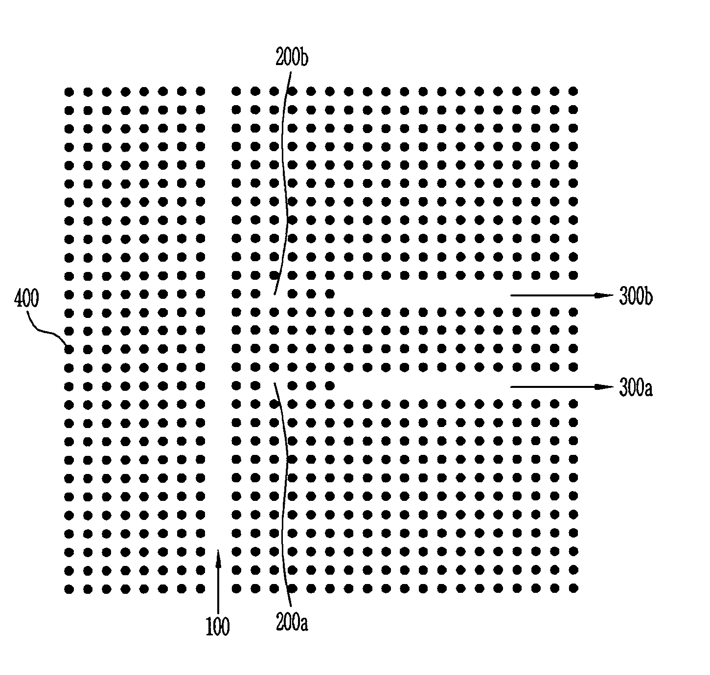
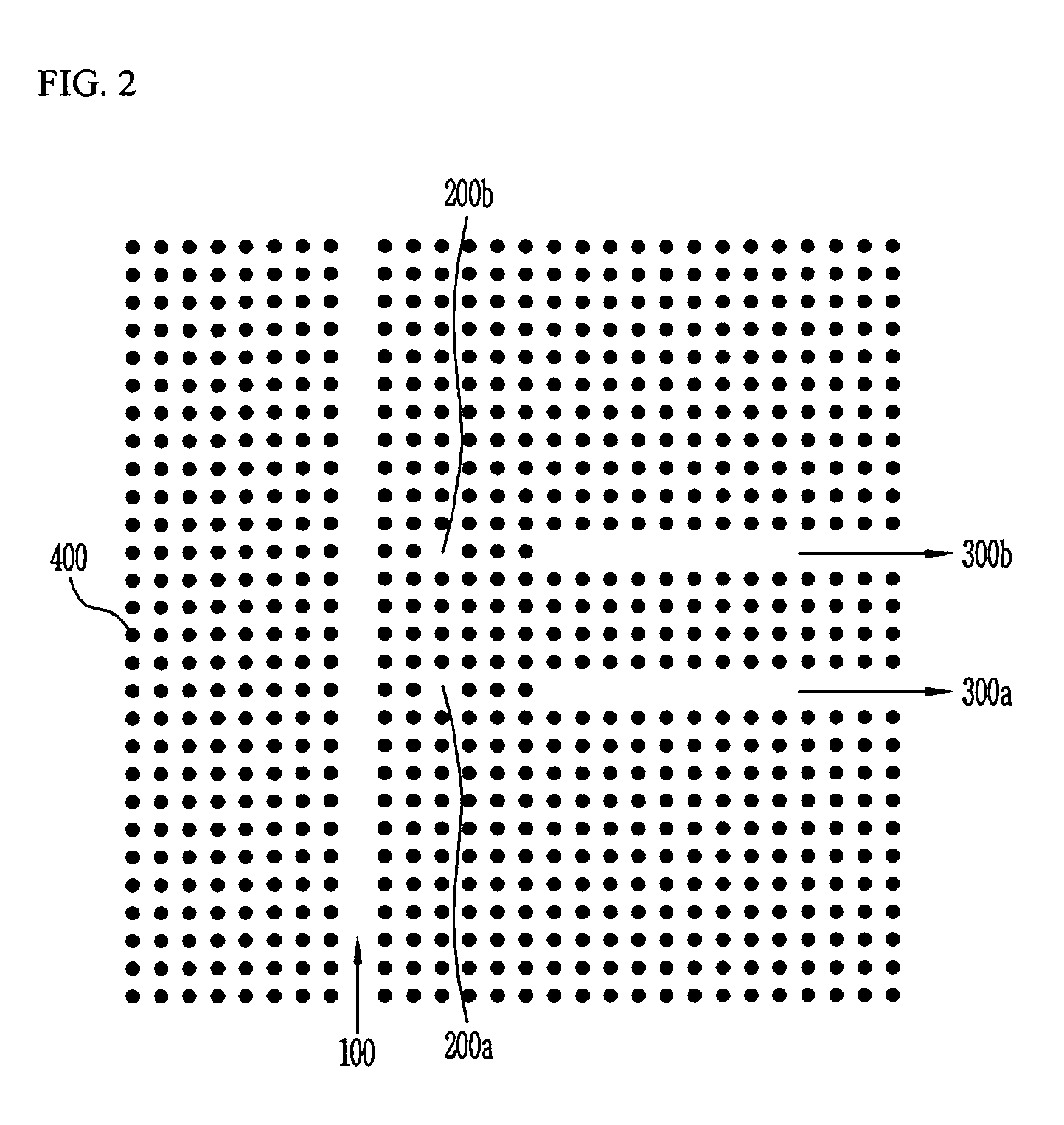
[0037] As described above, the present invention is directed to a multi-channel drop filter selecting light having a desired wavelength using a planar photonic crystal to filter the respective one in a direction perpendicular to the propagating direction. In the planar photonic crystal having dielectric rods periodically arranged or holes periodically bored in the dielectric thin film, light having a desired wavelength among light of various wavelengths guided along the bus wavelength is filtered through at least one resonator arranged between the bus waveguide and the drop waveguide, to the drop waveguide arranged perpendicular to the bus waveguide, thereby capable of being easily connected to the existing planar photonic crystal devices to enable fabrication by nanoimprint technology using an embossing process and to allow mass production at low costs as well as implementing an optical filter having an ultra narrowband line width and a high integrate...

Problems solved by technology

However, the conventional optical technology has a limitation in fulfilling the requirements in terms of performance and size of device.
However, in the afore-mentioned structure, the dropped light is guided along with the same drop waveguide so that it is not appropriate to the device such as DWDM, which should independently deal with the dropped light having different wavelengths from each other.
Therefore, there is a problem in that fabrication should be made in high precision.

Method used


Image

  • Multi-channel drop filter using photonic crystal
  • Multi-channel drop filter using photonic crystal
  • Multi-channel drop filter using photonic crystal

Examples


Embodiment Construction

[0019] Exemplary embodiments of the present invention will now be described in detail with reference to the accompanying drawings. However, the present invention is just illustrative, and should not be construed as limiting the scope of the present invention.

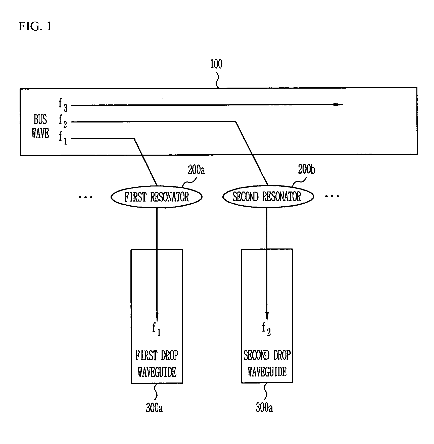
[0020]FIG. 1 is a schematic diagram illustrating a multi-channel drop filter using a photonic crystal according to an embodiment of the present invention.

[0021] As shown in FIG. 1, in the case that light having three frequencies (f1, f2, f3) is guided along one bus waveguide 100, the light having a frequency of f1 is dropped to a first drop waveguide 300a through a first resonator 200a, and the light having a frequency of f2 is dropped to a second drop waveguide 300b through a second resonator 200b.

[0022] With this principle, light of all frequencies or wavelengths guided along the bus waveguide 100 can be filtered to different drop waveguides from each other 300a and 300b.

[0023] In addition, filtering light having a desired...


PUM

PropertyMeasurementUnit
Wavelengthaaaaaaaaaa

Abstract

Provided is a multi-channel drop filter using a photonic crystal, wherein light having a desired wavelength among light of various wavelengths guided along a bus wavelength is filtered to the drop waveguide arranged perpendicular to the bus waveguide through a resonator arranged between the bus and drop waveguides, thereby being easily connected to the existing planar photonic crystal devices to enable fabrication by nanoimprint technology using an embossing process as well as implementing an optical filter having an ultra narrowband line width and a high integrated photonic integrated circuit.

Description

CROSS-REFERENCE TO RELATED APPLICATION [0001] This application claims priority to and the benefit of Korean Patent Application No. 2004-23303, filed on Apr. 6, 2004, the disclosure of which are incorporated herein by reference in its entirety. BACKGROUND [0002] 1. Field of the Invention [0003] The present invention relates to a multi-channel drop filter using a photonic crystal and, more specifically, to a multi-channel drop filter using a photonic crystal capable of being easily connected to an existing planar photonic crystal device and implementing an optical filter having an ultra narrowband line width and a high-density photonic integrated circuit, by forming a plurality of output waveguides, i.e., drop waveguides in a direction perpendicular to and near an input waveguide, i.e., a bus waveguide formed by a line defect within the photonic crystal as well as forming at least one resonator by a point defect between the bus waveguide and the drop waveguide. [0004] 2. Discussion of...

Claims


Application Information

Patent Timeline
IPC IPC(8): G02B6/293G02B6/10G02B6/12G02B6/122G02B6/28
CPCB82Y20/00G02B6/1225G02B6/12007B01D21/20B01D21/06C02F1/52
Inventor KEE, CHUL SIKHAN, SANG PILCHOI, CHOON GIYOON, KEUN BYOUNG
Owner ELECTRONICS & TELECOMM RES INST
Learn More