Spacer approach for CMOS devices

Inactive Publication Date: 2005-09-22
TAIWAN SEMICON MFG CO LTD
View PDF5 Cites 11 Cited by
  • Summary
  • Abstract
  • Description
  • Claims
  • Application Information

AI Technical Summary

Benefits of technology

[0007] These and other problems are generally reduced, solved or circumvented, and technical advantages are generally

Problems solved by technology

Significant challenges, however, are faced as the sizes of CMOS devices continue to decrease.
Consequently, a transistor with a short gate length suffers from problems related to the inability of the gate electrode to substantially control the on and off states of the channel.
The use of sacrificial spacers formed of TEOS, however, frequently causes damage to other oxide structures, such as, for example, shallow trench isolations (STIs).
When the sacrificial spacers formed of TEOS are removed, a portion or corner of the STI filler material may also be removed, which may adversely affect the electrical characteristics of the semiconductor devices, e.g., transistors, by increasing junction leakage at the edge of the STI.

Method used


Image

  • Spacer approach for CMOS devices
  • Spacer approach for CMOS devices
  • Spacer approach for CMOS devices

Examples


Embodiment Construction

[0013] The making and using of the presently preferred embodiments are discussed in detail below. It should be appreciated, however, that the present invention provides many applicable inventive concepts that can be embodied in a wide variety of specific contexts. Accordingly, the specific embodiments discussed herein are merely illustrative of specific ways to make and use the invention, and do not limit the scope of the invention.

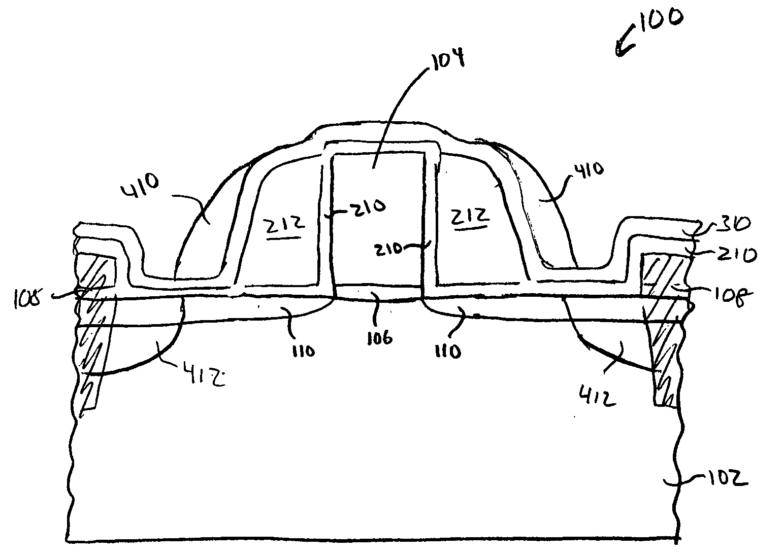
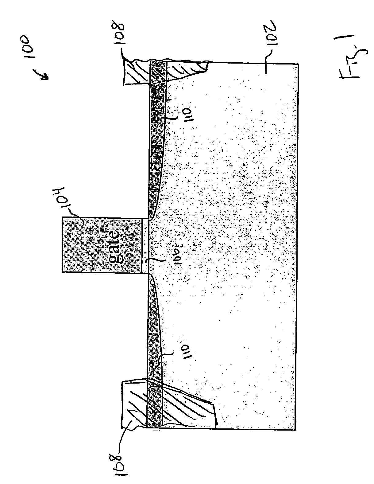
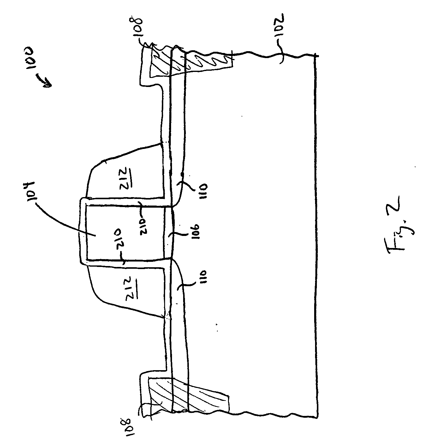
[0014] The invention described herein provides a method for forming a transistor characterized by good short channel control and avoiding damage to STIs or other structures. In particular, the method of the present invention described herein provides a method of forming graded source / drain regions to provide better short channel control using sacrificial spacers and etch stop layers. As will be discussed below, an etch stop layer is formed before the sacrificial spacers are formed and covers the STIs or other underlying structures. Materials used for the...


PUM


Abstract

A semiconductor device having a graded source / drain region for use in CMOS devices is provided. The semiconductor device is formed by utilizing a spacer and a sacrificial spacer as masks. The sacrificial spacer is formed over an etch stop layer, which acts as an etch stop and protects underlying structures from becoming damaged during the etching process. In particular, the present invention may be used, for example, to protect the edge or corner of a shallow trench isolation from becoming damaged during etching.

Description

TECHNICAL FIELD [0001] The present invention relates generally to semiconductor devices, and more particularly to a new spacer approach for use in fabricating complementary metal-oxide semiconductor (CMOS) devices. BACKGROUND [0002] Complementary metal-oxide-semiconductor (CMOS) technology is the dominant semiconductor technology used for the manufacture of ultra-large scale integrated (ULSI) circuits today. Size reduction of the semiconductor structures has provided significant improvement in the speed, performance, circuit density, and cost per unit function of semiconductor chips over the past few decades. Significant challenges, however, are faced as the sizes of CMOS devices continue to decrease. [0003] For example, as the length of the gate electrode of a CMOS transistor is reduced, the source and drain regions increasingly interact with the channel and gain influence on the channel potential and the gate dielectric. Consequently, a transistor with a short gate length suffers ...

Claims


Application Information

Patent Timeline
IPC IPC(8): H01L21/336H01L21/8238H01L29/78
CPCH01L29/6653H01L29/7833H01L29/6659H01L29/6656
Inventor CHANG, SUN-JAYWU, SHIEN-YANG
Owner TAIWAN SEMICON MFG CO LTD
Why Eureka
Try Eureka