Analog to digital converter circuit of successive approximation type operating at low voltage
- Summary
- Abstract
- Description
- Claims
- Application Information
AI Technical Summary
Benefits of technology
Problems solved by technology
Method used
Image
Examples
first preferred embodiment
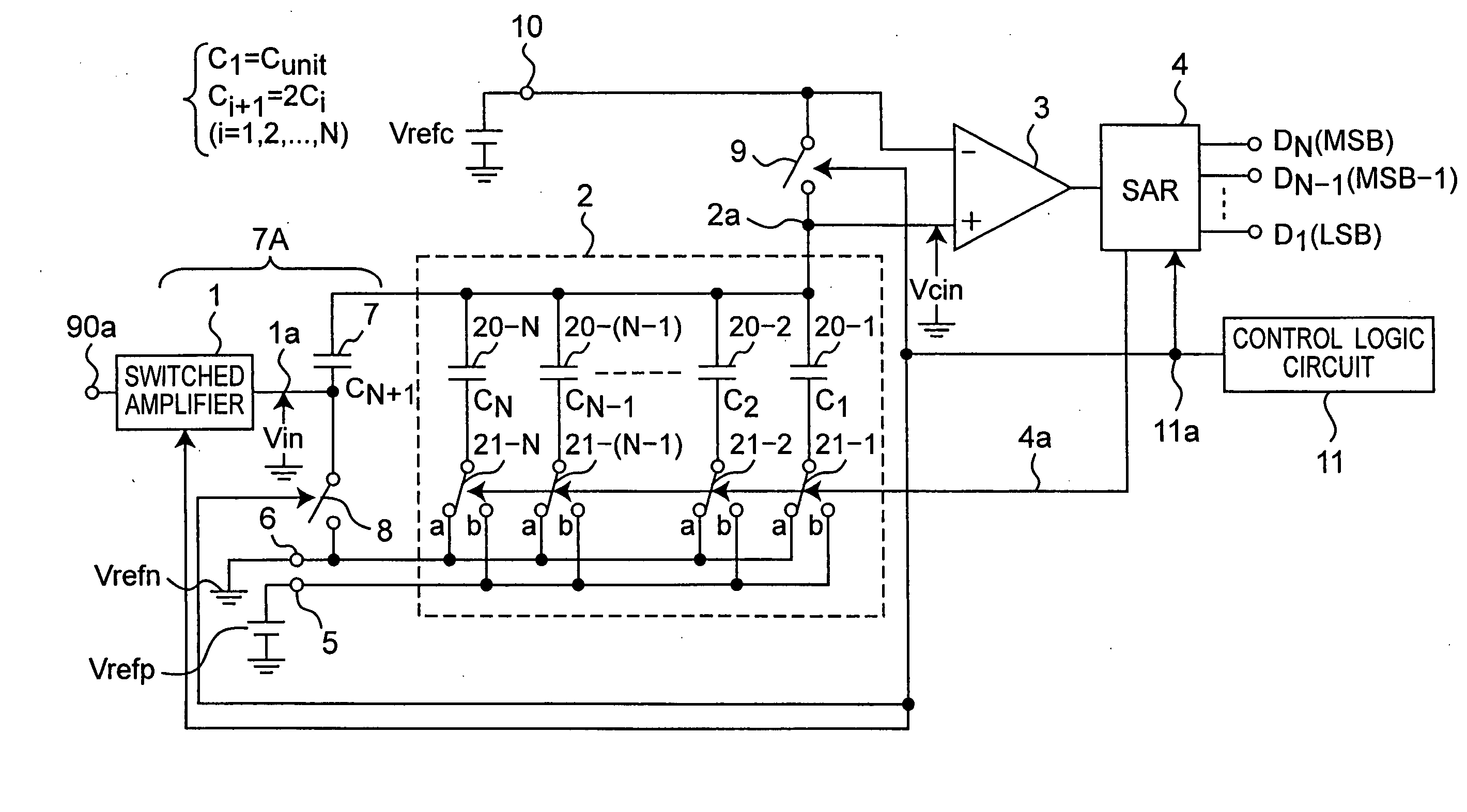
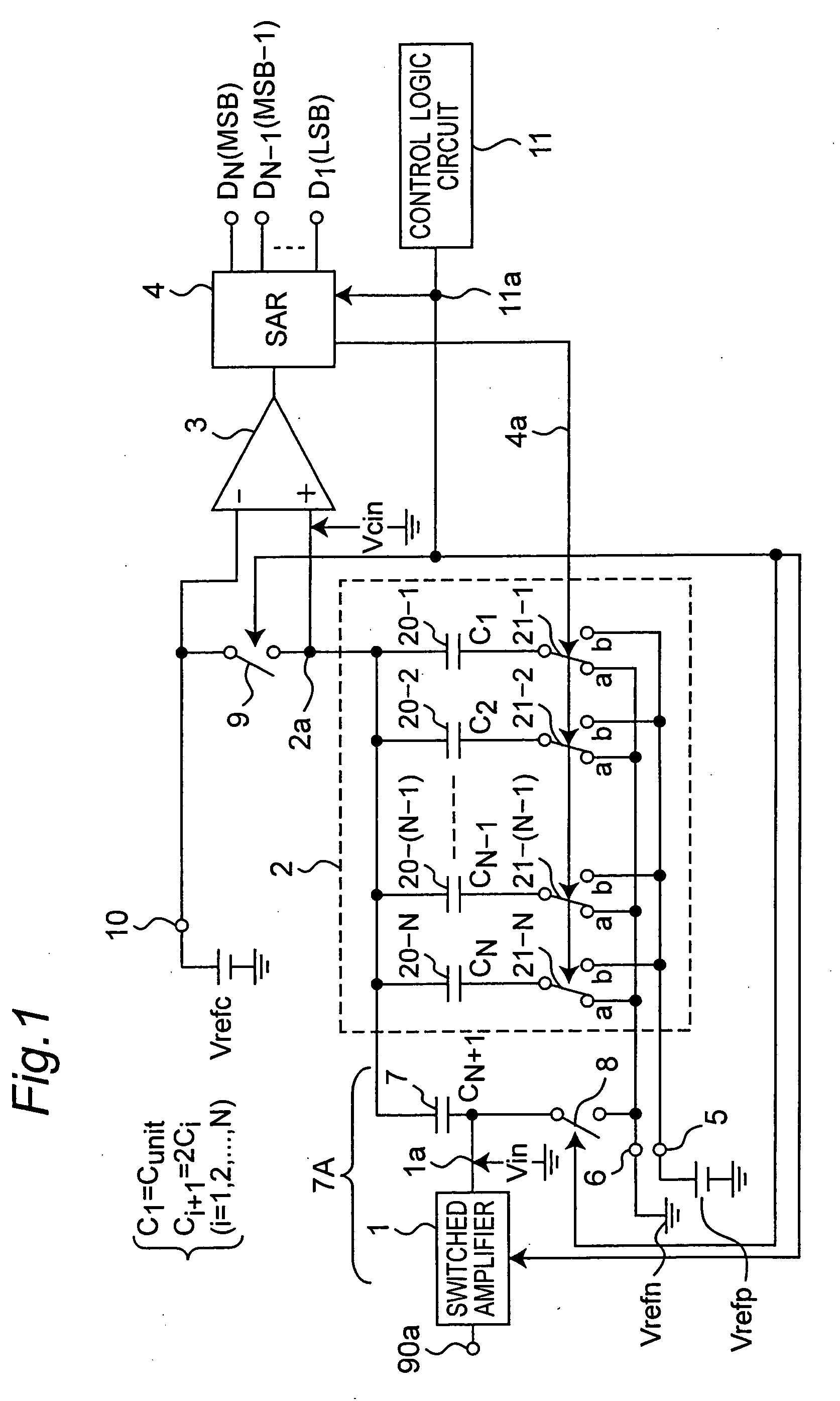
[0071]FIG. 1 is a circuit diagram showing a configuration of an AD converter circuit according to a first preferred embodiment of the present invention. The AD converter circuit according to the first preferred embodiment is an AD converter of successive approximation type that includes a local DA converter 2 using grounded switches each having one end connected to a ground potential (or a potential near the ground potential) Vrefn or a reference voltage source Vrefp, a sample hold circuit 7A as configured by a switched amplifier 1 and a hold capacitor 7, and a comparator 3 as configured to be simpler to have a less wide common-mode input voltage range than that of the prior art examples. The AD converter circuit according to the first preferred embodiment is characterized by being able to operate at a power supply voltage Vdd equal to or lower than 1 V.
[0072] Referring to FIG. 1, the switched amplifier 1 samples an input analog signal inputted via an input analog signal terminal 9...
second preferred embodiment
[0102]FIG. 15 is a circuit diagram showing a configuration of an AD converter circuit according to a second preferred embodiment of the present invention. The AD converter circuit according to the second preferred embodiment is characterized, as compared with that according to the first preferred embodiment, in that a voltage polarity of each of the capacitors 20-1 to 20-N is inverted, one end of the hold capacitor 7 is connected to the terminal 5 via the switch 8, and in that during sampling and holding, after lower one end of each of the capacitors 20-1 to 20-N is connected to the reference voltage source Vrefp, a successive approximation process of a control logic circuit 11A is performed as described below in detail by increasing voltages of sampled values, then successively reducing the voltages, and then making a comparison during successive approximation.
[0103] In an AD converter circuit of successive approximation type shown in FIG. 15, an input analog signal is sampled by ...
third preferred embodiment
[0106]FIG. 16 is a circuit diagram showing a configuration of an AD converter circuit according to a third preferred embodiment of the present invention. The AD converter circuit according to the third preferred embodiment is characterized, as compared with that according to the first preferred embodiment shown in FIG. 1, by further including an additional capacitor 12 having a capacitance Cs between a connection line of an output voltage 2a from the DA converter 2 and the terminal 5. In the AD converter circuit according to the third preferred embodiment as configured as described above, the additional hold capacitor 12 can control the maximum amplitude of the output voltage Vcin from the DA converter 2. If the additional hold capacitor 12 is not provided (in case of FIG. 1), and the output voltage from the DA converter 2 is defined as a voltage Vcin and that the output voltage of the switched amplifier 1 is defined as a voltage Vin, then the output voltage Vin is represented by th...
PUM
 Abstract
Description
Claims
Application Information
 - R&D
- Intellectual Property
- Life Sciences
- Materials
- Tech Scout
- Unparalleled Data Quality
- Higher Quality Content
- 60% Fewer Hallucinations
Browse by: Latest US Patents, China's latest patents, Technical Efficacy Thesaurus, Application Domain, Technology Topic, Popular Technical Reports.
© 2025 PatSnap. All rights reserved.Legal|Privacy policy|Modern Slavery Act Transparency Statement|Sitemap|About US| Contact US: help@patsnap.com


