Optical compensation film and liquid crystal display
- Summary
- Abstract
- Description
- Claims
- Application Information
AI Technical Summary
Benefits of technology
Problems solved by technology
Method used
Image
Examples
example 1
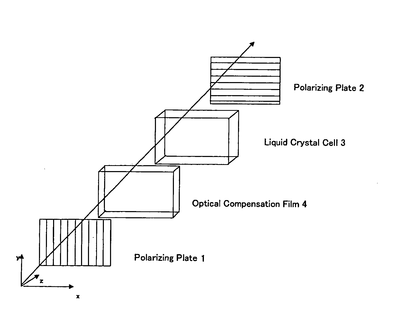
[0244] An optical simulation was carried out with respect to a liquid-crystal display model, having a same configuration as shown in FIG. 7, to confirm the effect of the present invention. For optical calculations, “LCD Master Ver6.08” provided by Shintech, INC. was used. A liquid crystal cell, electrodes, substrates polarizing plates or the like employed in known liquid crystal displays can be applied to the model. The postulated model had a liquid crystal cell, employing a vertical alignment with 90° pre-tilt angle, in which the cell gap was determined such that retardation of the liquid crystal cell (i.e., product Δn·d of the thickness d (μm) and refractive index anisotropy Δn) was 300 nm. As the values relating to a polarizing film, the values of “G1220DU”, which were input preliminarily into a simulator, were used. The retardation, Re and Rth, values at 450 nm, 550 nm and 650 nm of the optical compensation film, were set as shown in the columns for Liquid crystal display No. 1 ...
example 2
[0248] Using a liquid crystal display model having a similar configuration to as shown in FIG. 7, or in other words comprising an upper polarizing plate (protective film (not shown), polarizing film 1), an optical compensation film 5 (also serves as the protective film 3a), a liquid crystal cell (upper substrate 6, a liquid crystal layer 7, a lower substrate 8), an optical compensation film 9 (also serves as the protective film 103a) and a lower polarizing plate (polarizing film 101, protective film (not shown)) stacked in this order as viewed from the direction of viewing (top), and a back light source (not shown), the simulation was carried out in the same manner as Example 1. The retardation, Re and Rth, values at 450 nm, 550 nm and 650 nm of the optical compensation film, were varied as shown in the columns for Liquid crystal display Nos. 7 to 12 in Table 2 shown below. Other conditions were set as same as the above. And, thus, the transmittances (%) and the color shifting value...
example 3
[0249] Using a liquid crystal display having a similar configuration to as shown in FIG. 7 except that an optical compensation film 5 is absent, or in other words comprising an upper polarizing plate (protective film (not shown), a polarizing film 1, a protective film 3a), a liquid crystal cell (upper substrate 6, liquid crystal layer 7, a lower substrate 8), an optical compensation film 9 (also serves as the protective film 103a) and a lower polarizing plate (polarizing film 101, protective film (not shown)) stacked in this order as viewed from the direction of viewing (top), and a back light source (not shown), the simulation was carried out in the same manner as Example 1. The retardation, Re and Rth, values at 450 nm, 550 nm and 650 nm of an optical compensation film, were varied as shown in the columns for Liquid crystal display Nos. 13 to 18 in Table 3 shown below. Other conditions were set as same as the above. And, thus, the transmittances (%) and the color shifting values w...
PUM
 Abstract
Description
Claims
Application Information
 - R&D
- Intellectual Property
- Life Sciences
- Materials
- Tech Scout
- Unparalleled Data Quality
- Higher Quality Content
- 60% Fewer Hallucinations
Browse by: Latest US Patents, China's latest patents, Technical Efficacy Thesaurus, Application Domain, Technology Topic, Popular Technical Reports.
© 2025 PatSnap. All rights reserved.Legal|Privacy policy|Modern Slavery Act Transparency Statement|Sitemap|About US| Contact US: help@patsnap.com


