Transferring semiconductor crystal from a substrate to a resin

a technology of semiconductor crystals and resins, applied in the field of electronic parts, can solve the problems of unnecessary cost increase, unfavorable current concentration, increase in internal resistance, etc., and achieve the effect of reducing production costs, facilitating electronic parts mounting, and increasing the number of devices formed from a single sheet of crystalline wafers

Inactive Publication Date: 2005-08-25
SONY CORP
View PDF14 Cites 5 Cited by
  • Summary
  • Abstract
  • Description
  • Claims
  • Application Information

AI Technical Summary

Benefits of technology

[0010] The present invention has been proposed in consideration of the above situations in the related art. Accordingly, it is an object of the present invention to provide an electronic part in which the number of devices formed from a single sheet of crystalline wafer can be enlarged as compared with the conventional packaged devices, production cost can be reduced, and it is easy to mount the electronic part in high density, and a method of producing the same. In addition, it is another object of the present invention to provide a large-type system, a high-performance system, and a system based on integration of a different kinds of devices (for example, image display system), which cannot be realized with a system based on integration of a multiplicity of devices produced by a monolithic process.
[0012] In the electronic part having the above-mentioned structure, the region necessary for actual mounting and leading-out of electrodes is minimized, and the overall size of the device is suppressed to be small. In addition, for example, in the case of a light-emitting diode, a laser diode, or the like produced by epitaxial growth of a gallium nitride based crystal on a sapphire substrate, such problems as an increase in internal resistance and unfavorable concentration of current are dissolved. In the case of a light-emitting diode including an aluminum gallium indium phosphide based crystal grown on a gallium arsenide substrate, high light emission efficiency is realized, and such contrivances that may cause a rise in cost are unnecessary.
[0014] According to the image display system and the method of manufacturing the same, the light-emitting devices rearranged in the spaced-apart condition are arranged in a matrix form to constitute an image display portion. Therefore, the light-emitting devices produced by fine processing with a dense condition, namely, with a high degree of integration can be efficiently rearranged in the spaced-apart condition, and productivity is largely enhanced. In addition, the light-emitting devices converted into electronic parts can be actually mounted in a high density, and wiring therefor can be easily formed.
[0015] According to the present invention, it is possible to provide an electronic part such that the number of devices produced from a single sheet of crystal wafer can be enlarged as compared with the conventional packaged devices, the production cost can be reduced, and actual mounting in a high density is easy. In addition, it is possible to provide a large-type system, a high-performance system, and a system based on integration of different kinds of devices (for example, an image display system), which cannot be realized with a system based on integration of a multiplicity of devices produced by a monolithic process. On the other hand, according to the image display system and the method of manufacturing the same according to the present invention, while the above-mentioned merits are maintained, the light-emitting devices produced by fine processing with a dense condition, namely, with a high degree of integration can be efficiently rearranged with the spaced-apart condition. Therefore, an image display system with high accuracy can be produced with high productivity.

Problems solved by technology

In addition, for example, in the case of a light-emitting diode, a laser diode, or the like produced by epitaxial growth of a gallium nitride based crystal on a sapphire substrate, such problems as an increase in internal resistance and unfavorable concentration of current are dissolved.
In the case of a light-emitting diode including an aluminum gallium indium phosphide based crystal grown on a gallium arsenide substrate, high light emission efficiency is realized, and such contrivances that may cause a rise in cost are unnecessary.

Method used


Image

  • Transferring semiconductor crystal from a substrate to a resin
  • Transferring semiconductor crystal from a substrate to a resin
  • Transferring semiconductor crystal from a substrate to a resin

Examples


Embodiment Construction

[0057] Now, an electronic part and a method of producing an electronic part by application of the present invention, and further, an image display system and a method of manufacturing an image display system by application thereof will be described in detail below referring to the drawings.

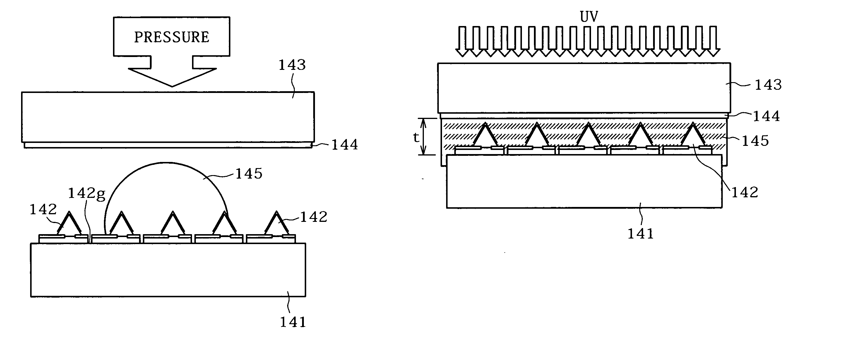
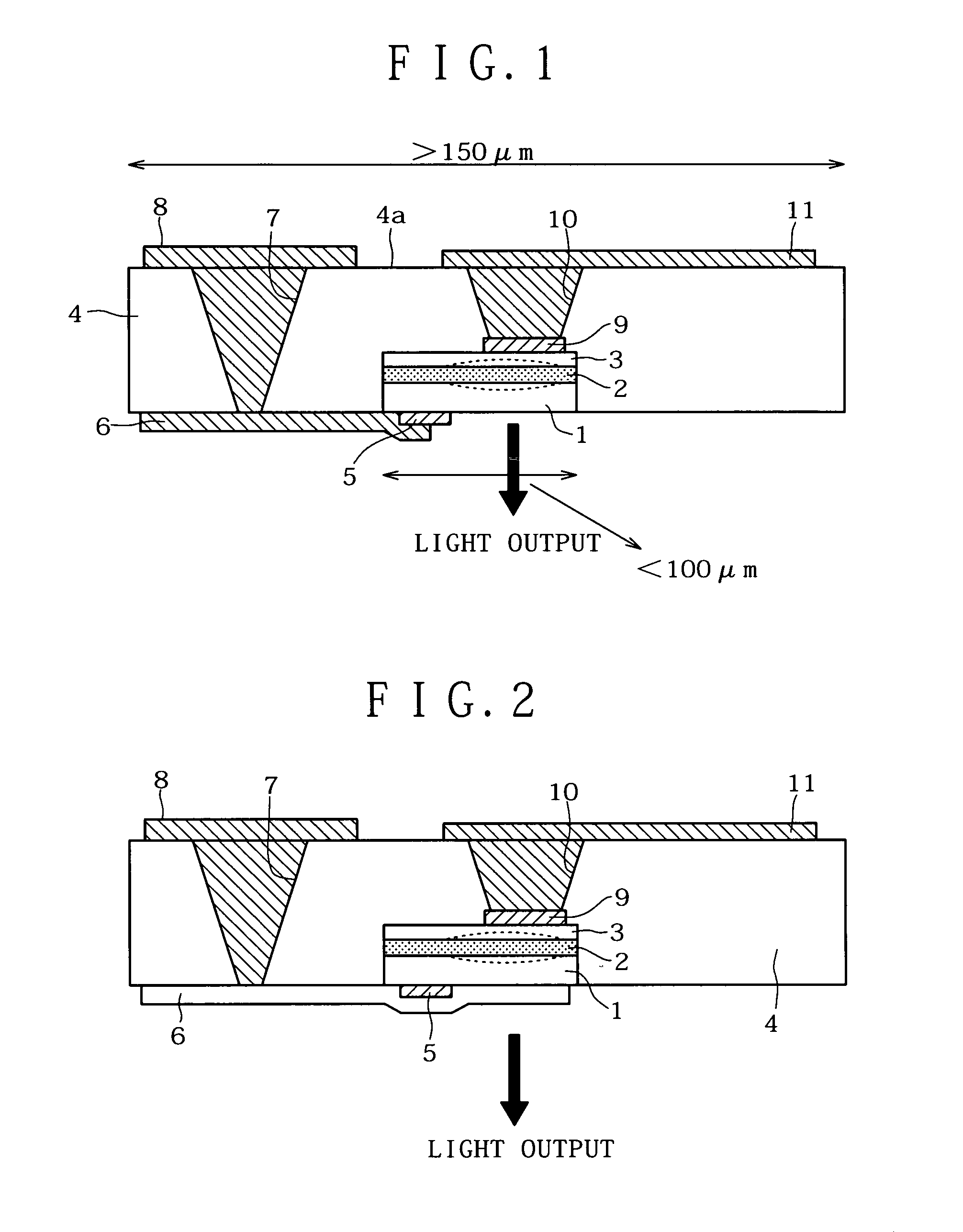
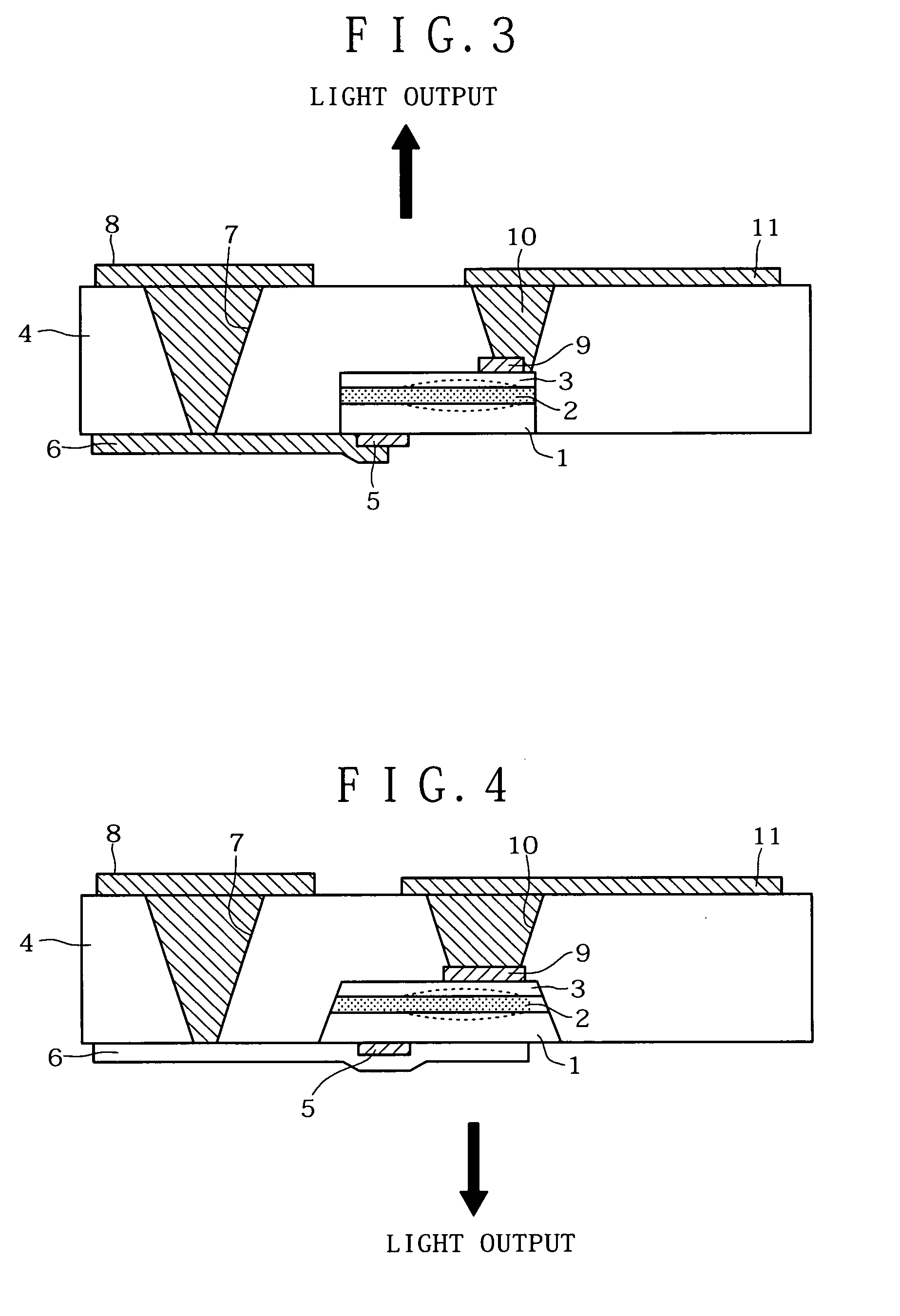
[0058]FIG. 1 shows an example in which the present invention is applied to a gallium nitride based light-emitting diode. The light-emitting diode is composed of an n-GaN window layer 1 epitaxially grown on a sapphire substrate, a GaInN active layer 2, and a p-GaN clad layer 3. These semiconductor crystal layers are embedded in a resin layer 4. The size of the semiconductor crystal layer is, for example, not more than 100 μm square, and the size of the resin layer 4 is, for example, not less than 150 μm square. Of the GaInN active layer 2, the region surrounded by the broken line is an active region, and a light output in the direction of the arrow is obtained.

[0059] The n-GaN window layer 1 is e...


PUM


Abstract

A semiconductor crystal layer formed by epitaxial growth on a seed crystal substrate is embedded in an insulating material in the condition where the seed crystal substrate is removed, electrodes are provided respectively on a first surface of the semiconductor crystal layer and a second surface of the semiconductor layer opposite to the first surface, and lead-out electrodes connected to the electrodes are led out to the same surface side of the insulating material. The semiconductor crystal layer functions as a semiconductor light-emitting device or a semiconductor electronic device. The insulating material is, for example, a resin.

Description

CROSS REFERENCE TO RELATED APPLICATIONS [0001] This application is a Continuation of application Ser. No. 10 / 894,771, filed on Jul. 20, 2004, entitled TRANSFERRING SEMICONDUCTOR CRYSTAL FROM A SUBSTRATE TO A RESIN which, in turn, is a Divisional of prior application Ser. No. 10 / 308,914, filed on Dec. 3, 2002, entitled TRANSFERRING SEMICONDUCTOR CRYSTAL FROM A SUBSTRATE TO A RESIN (now U.S. Pat. No. 6,770,960) which, in turn, claims priority to Japanese application No. JP2001-368570 filed Dec. 3, 2001.BACKGROUND OF THE INVENTION [0002] The present invention relates to an electronic part including as an active device a semiconductor crystal layer formed by epitaxial growth on a seed crystal substrate, and a method of producing the same. Furthermore, the present invention relates to an image display system including such electronic parts, and a method of manufacturing the same. [0003] In the case of arranging light-emitting devices in a matrix form to assemble an image display system, ...

Claims


Application Information

Patent Timeline
Patent Type & Authority Applications(United States)
IPC IPC(8): H01L21/205G09F9/33H01L21/338H01L21/60H01L23/12H01L25/075H01L29/812H01L33/14H01L33/30H01L33/34H01L33/54H01L33/56H01L33/62H01S5/02H01S5/02315H01S5/042H01S5/183
CPCH01L24/24H01L24/82H01L2924/1306H01L25/0753H01L33/54H01L33/62H01L2221/68368H01L2224/24137H01L2224/24226H01L2924/01012H01L2924/01013H01L2924/01015H01L2924/01039H01L2924/01046H01L2924/01049H01L2924/01057H01L2924/01078H01L2924/01079H01L2924/01082H01L2924/10329H01L2924/1033H01L2924/10349H01S5/02H01S5/02228H01S5/02236H01S5/0425H01S5/183H01L2924/01005H01L2924/01006H01L2924/01033H01L2924/12041H01L2924/00H01L2924/12042H01S5/04257H01S5/32325H01L2224/24H01S5/04253H01S5/04256H01L2224/04105H01L2224/96H01S5/02234H01S5/0233H01S5/0235H01S5/02315H01L2924/00012
Inventor OOHATA, TOYOHARU
Owner SONY CORP
Why Eureka
Try Eureka