Semiconductor device

a technology semiconductors, applied in the direction of semiconductor devices, basic electric elements, electrical equipment, etc., can solve the problems of high-speed operation, inability to reduce capacitance, and inability to make progress in the reduction of schottky barrier diodes

Inactive Publication Date: 2005-08-25
SANYO ELECTRIC CO LTD
View PDF2 Cites 10 Cited by
  • Summary
  • Abstract
  • Description
  • Claims
  • Application Information

AI Technical Summary

Benefits of technology

[0049] According to the embodiment of the invention, since the expansion of the depletion layer becomes uniform at the end and near the center of the Schottky junction region, it is possible to obtain a stable breakdown voltage.
[0050] Since an oxide film (the trench) is provided to reach the n+ type substrate, the depletion layer expanding to the periphery of the guard ring in the conventional technique is eliminated to make it possible to realize a reduction in capacitance.
[0051] Moreover, since the p+ type region constituting the guard ring is made unnecessary, holes are never injected when the forward voltage is applied. In other words, since carriers are not accumulated, it is unnecessary to perform the outflow or the recombination of holes. Therefore, since the reverse recovery time (Trr) is not required, it is possible to improve switching operation speed. More specifically, it is possible to improve the switching operation speed, which is several hundreds ns in the conventional technique, to about several tens ns. In addition, since a loss at the switching time is eliminated, set efficiency is improved.

Problems solved by technology

Since the depletion layer 50′ becomes a capacitance component, there is a problem in that a reduction in capacitance of the Schottky barrier diode does not make progress.
In addition, there is also a problem in that the guard ring 15 prevents a high-speed operation.
There is a problem in that the reduction in capacitance does not make progress and the high-speed operation is prevented by providing the guard ring for securing a breakdown voltage.

Method used


Image

  • Semiconductor device
  • Semiconductor device
  • Semiconductor device

Examples


Embodiment Construction

[0027] An embodiment of the invention will be explained in detail with reference to FIGS. 1A and 1B to FIGS. 3A to 3C.

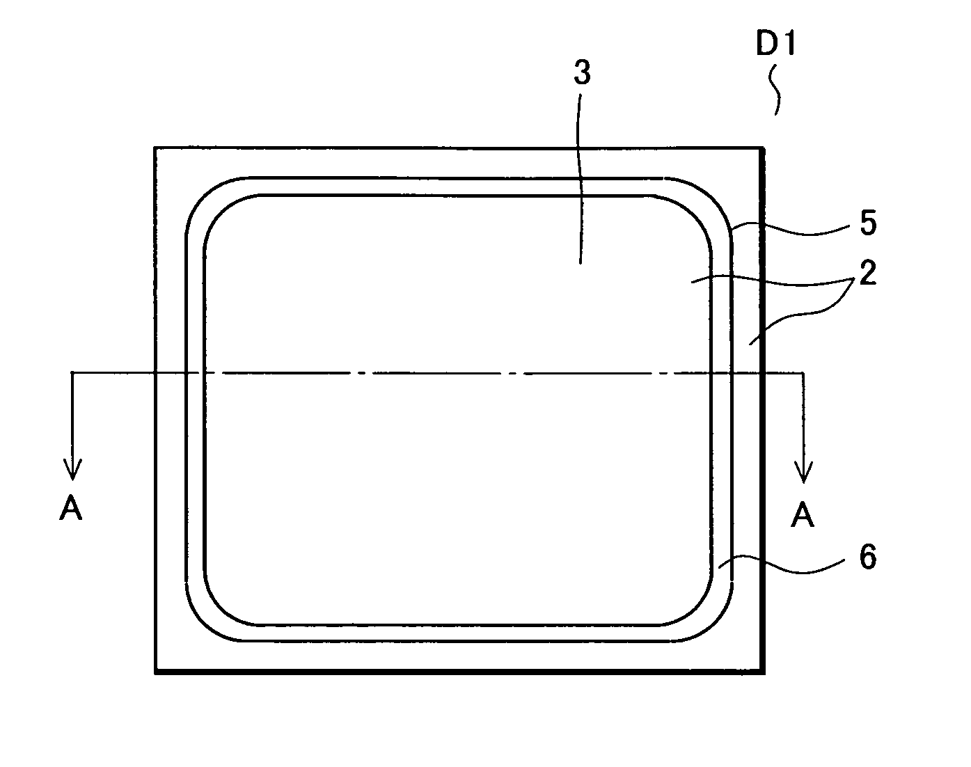
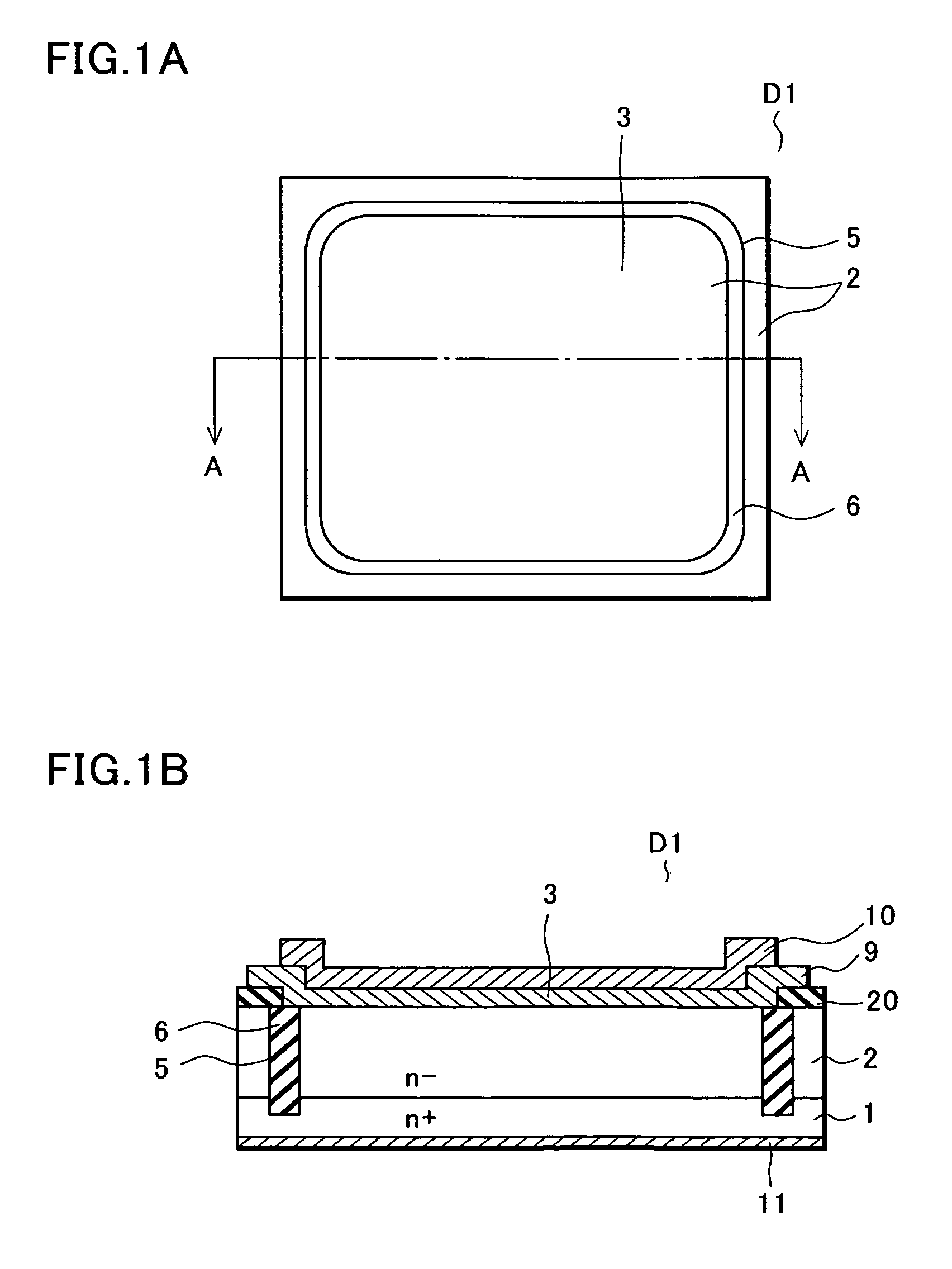
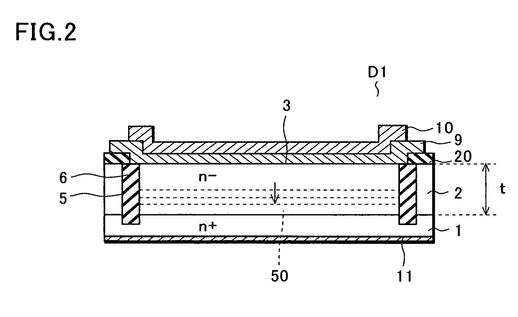
[0028]FIGS. 1A and 1B show a Schottky barrier diode D1 according to the embodiment of the invention. FIG. 1A is a plan view of the Schottky barrier diode D1 and FIG. 1B is a sectional view along line A-A in FIG. 1A. Note that a Schottky metal layer and an anode electrode on a surface of the Schottky barrier diode D1 are not shown in FIG. 1A.

[0029] The Schottky barrier diode D1 according to the embodiment of the invention includes a one conduction type semiconductor substrate 1, a one conduction type semiconductor layer 2, a trench 5, an insulating film 6, and a Schottky metal layer 9.

[0030] A substrate is obtained by stacking the n− type semiconductor layer 2 on the n+ type silicon semiconductor substrate 1 according to, for example, epitaxial growth.

[0031] The Schottky metal layer 9 made of Mo or the like, which forms a Schottky junction with a surface of the n−...


PUM


Abstract

Conventionally, a guard ring for securing a breakdown voltage is provided around a Schottky barrier diode. Since the guard ring is a p+ type region, a depletion layer expands around the guard ring when a reverse voltage is applied to prevent a reduction in capacitance. In addition, there is a problem in that, when a forward voltage is applied, holes are injected from the guard ring if the applied voltage exceeds a predetermined voltage and high-speed operation cannot be realized. To solve the problems, a trench is provided in a guard ring region of the conventional technique and an insulating film is provided inside the trench. The trench is provided to reach an n+ type semiconductor substrate. Consequently, since the depletion layer expands only in a depth direction until the depletion layer reaches the n+ type semiconductor substrate, it is possible to realize a reduction in capacitance. In addition, since the p+ type region is made unnecessary, a reverse recovery time (Trr) does not occur. Therefore, it is possible to improve switching operation speed.

Description

BACKGROUND OF THE INVENTION [0001] 1. Field of the Invention [0002] The present invention relates to a semiconductor device, and in particular to a semiconductor device that realizes a reduction in capacitance and high-speed switching of a Schottky barrier diode. [0003] 2. Description of the Related Art [0004]FIGS. 4A and 4B show a conventional Schottky barrier diode D2. FIG. 4A is a plan view of the Schottky barrier diode D2 and FIG. 4B is a sectional view along line B-B in FIG. 4A. Note that Schottky metal layer and an anode electrode are not shown in the diagram view. [0005] A substrate is obtained by stacking an n− type epitaxial layer 12b on an n+ type semiconductor substrate 12a. A metal layer 13, which forms a Schottky junction with the n− type epitaxial layer 12b, is provided on a surface of the n− type epitaxial layer 12b. The metal layer 13 is made of, for example, Mo. The metal layer 13 is provided in the opening of an insulating film 30 formed on the surface of the n− ty...

Claims


Application Information

Patent Timeline
IPC IPC(8): H01L29/00H01L29/06H01L29/47H01L29/872
CPCH01L29/0619H01L29/872H01L29/0692H01L29/0649H01L29/47
Inventor OKADA, TETSUYA
Owner SANYO ELECTRIC CO LTD
Why Eureka
Try Eureka