Exposure apparatus and device manufacturing method
a technology of exposure apparatus and manufacturing method, which is applied in the direction of instruments, printers, therapy, etc., can solve the problems of reducing the yield of device production and deteriorating the reliability of devi
- Summary
- Abstract
- Description
- Claims
- Application Information
AI Technical Summary
Benefits of technology
Problems solved by technology
Method used
Image

Examples
embodiment 1
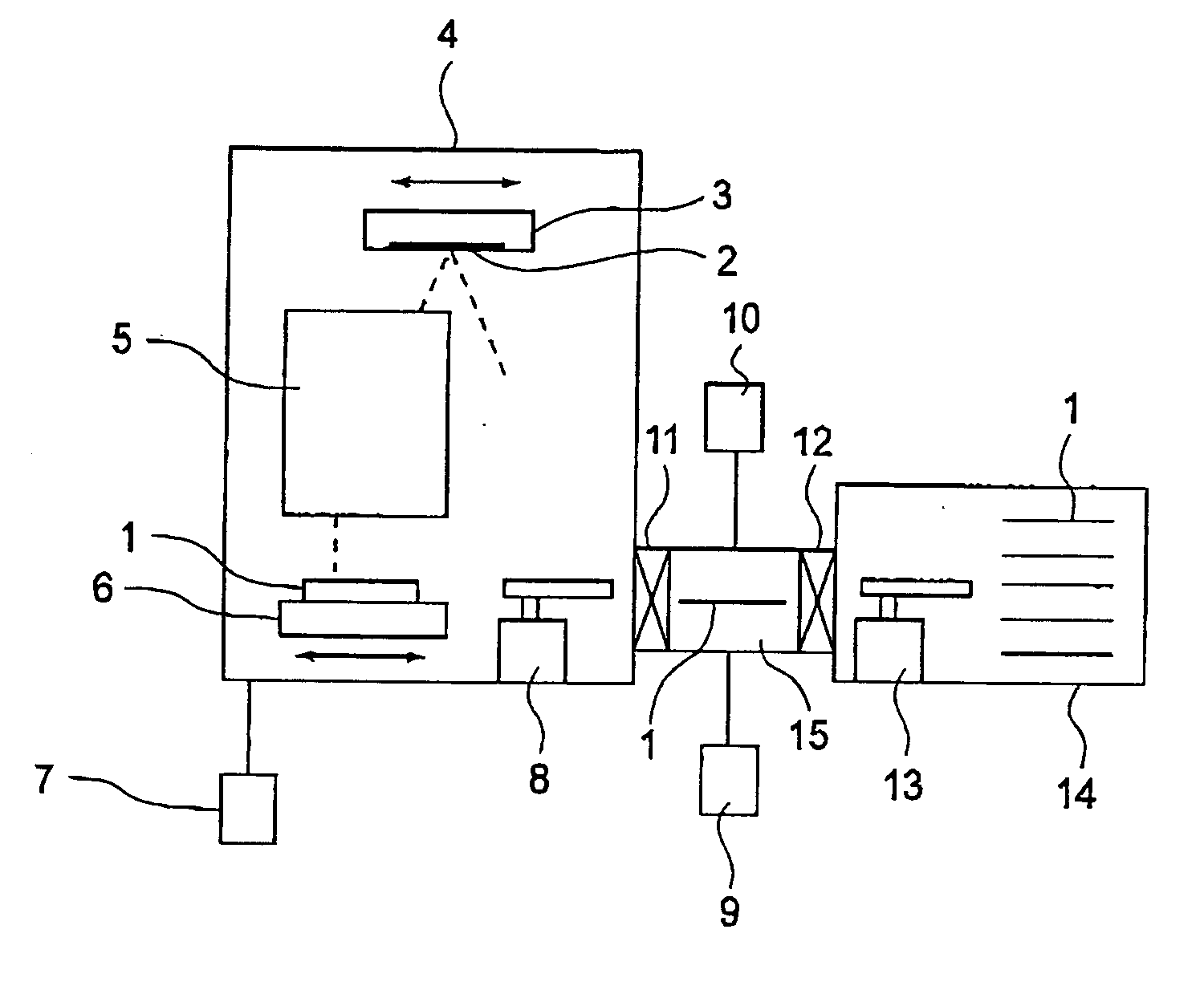
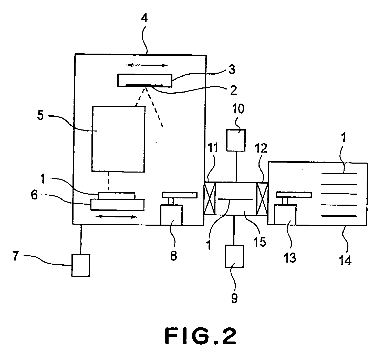
[0048] First of all, a projection exposure apparatus to which the present invention is applied will be explained, with reference to an EUV exposure apparatus shown in FIG. 2 of the drawings.
[0049] In FIG. 2, denoted at 1 is a wafer, and denoted at 2 is a reflection type mask having n electronic circuit pattern formed thereon. Denoted at 3 is a mask stage for holding a reflection type mask thereon and for coarsely and finely moving the same in a scan direction, and denoted at 5 is an optical system for directing reflection light from the mask to a wafer 1 for projection exposure thereof. Denoted at 6 is a wafer stage for holding a wafer thereon and for coarsely and finely moving the same in six-axis directions. The position of the wafer stage with respect to X- and Y-axis directions is continuously monitored by means of laser interferometers (not shown). Normally, the scan motion of the mask stage 3 and the wafer stage 6 is synchronously controlled to assure that, where the reductio...
embodiment 2
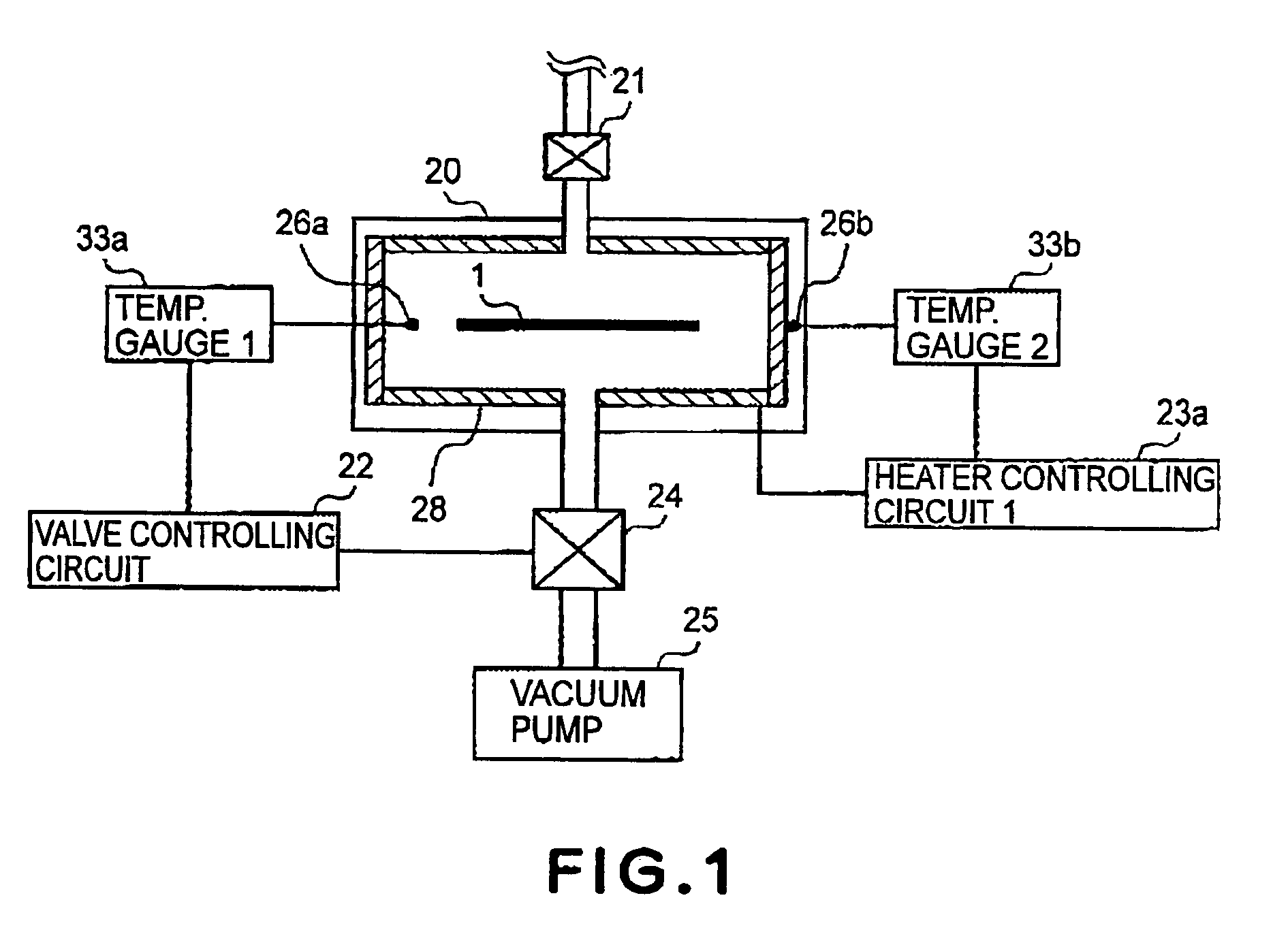
[0078] A second embodiment of the present invention pays a specific note to the throughput. As an important feature, in relation to the supply of a vent gas into the chamber, a gas heating mechanism is provided separately from the load-lock chamber wall heating means, thereby to assure that a gas having a temperature raised beforehand up to a predetermined temperature is supplied into the chamber. This enables initiation of vacuum evacuation just after the wafer exchange.
[0079] Referring to FIG. 16, this embodiment will be described in detail. This embodiment differs from the first embodiment in that there is a heat exchanger 35 at an upstream position of a vent valve 21. The heat exchanger comprises a heater and a large number of fins connected thereto. Disposed downstream of this heat exchanger is a sensor 26c for measuring the gas temperature, the sensor being provided in a pipe. In association with a temperature gauge 3 (33c), the temperature of the heated gas can be measured. ...
embodiment 3
[0083] Next, referring to FIGS. 21 and 22, an embodiment of a device manufacturing method which uses an exposure apparatus described above, will be explained.
[0084]FIG. 21 is a flow chart for explaining the procedure of manufacturing various microdevices such as semiconductor chips (e.g., ICs or LSIs), liquid crystal panels, or CCDS, for example. Step 1 is a design process for designing a circuit of a semiconductor device. Step 2 is a process for making a mask on the basis of the circuit pattern design. Step 3 is a process for preparing a wafer by using a material such as silicon. Step 4 is a wafer process which is called a pre-process wherein, by using the thus prepared mask and wafer, a circuit is formed on the wafer in practice, in accordance with lithography. Step 5 subsequent to this is an assembling step which is called a post-process wherein the wafer having been processed at step 4 is formed into semiconductor chips. This step includes an assembling (dicing and bonding) pro...
PUM
| Property | Measurement | Unit |
|---|---|---|
| temperature | aaaaa | aaaaa |
| temperature | aaaaa | aaaaa |
| temperature | aaaaa | aaaaa |
Abstract
Description
Claims
Application Information
 - Generate Ideas
- Intellectual Property
- Life Sciences
- Materials
- Tech Scout
- Unparalleled Data Quality
- Higher Quality Content
- 60% Fewer Hallucinations
Browse by: Latest US Patents, China's latest patents, Technical Efficacy Thesaurus, Application Domain, Technology Topic, Popular Technical Reports.
© 2025 PatSnap. All rights reserved.Legal|Privacy policy|Modern Slavery Act Transparency Statement|Sitemap|About US| Contact US: help@patsnap.com