
Electrostatic discharge guide and liquid crystal display utilizing same

a liquid crystal display and electrostatic discharge technology, which is applied in the direction of optics, instruments, electrical equipment, etc., can solve the problems of damage to the circuit or device therein, damage to the entire system, and electrostatic charge that is not released in some way to the tft-lcd

Active Publication Date: 2005-08-18
AU OPTRONICS CORP
View PDF5 Cites 14 Cited by
  • Summary
  • Abstract
  • Description
  • Claims
  • Application Information

AI Technical Summary

Benefits of technology

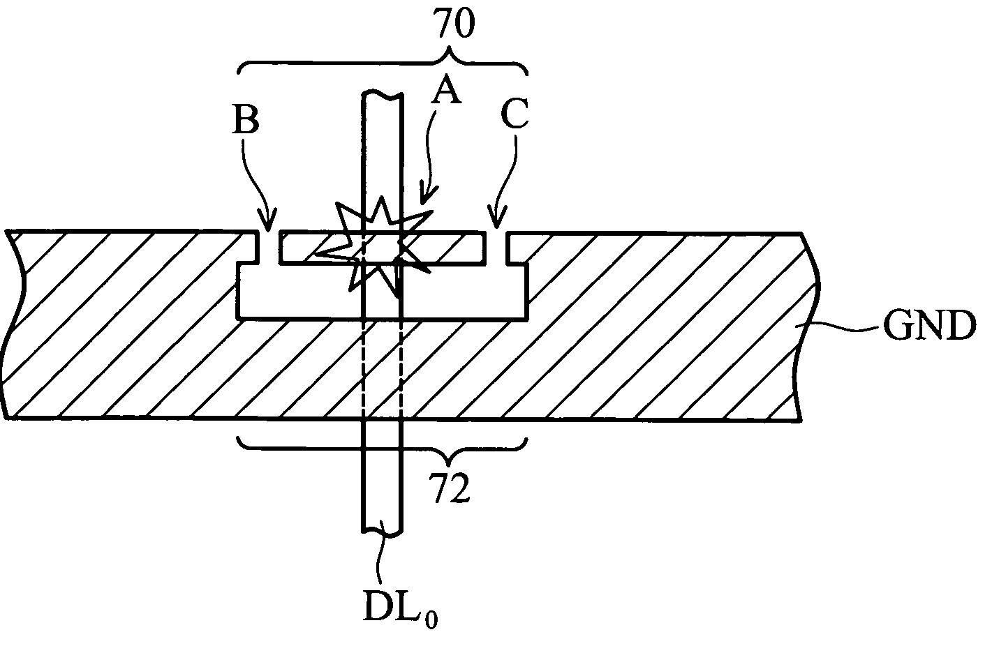
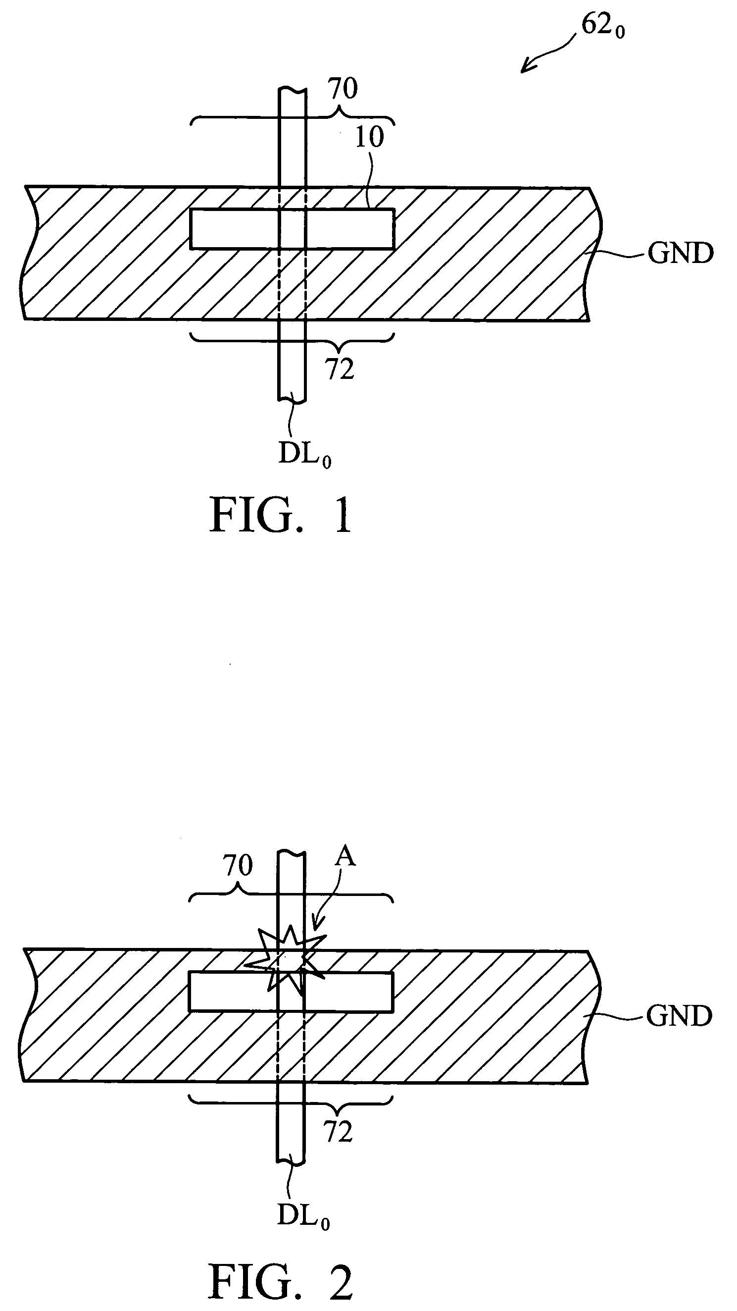
"The present invention provides a structure for guiding electrostatic discharge to a specific location. This is achieved by using an ESD guide comprising a ground wire, isolated from a data line, with at least one main ground segment and at least one electrostatic discharge triggering segment connected to the main ground segment. The electrostatic discharge triggering segment comprises two ends connected with the main ground segment. The ground wire further comprises an opening substantially surrounded by the main ground segment and the electrostatic discharge triggering segment and intersecting the data line. The present invention also provides a liquid crystal display with an ESD guide. The technical effects of this invention include reducing the risk of electrostatic discharge damage to the data lines and improving the reliability of the display."

Problems solved by technology

Electrostatic discharge, abbreviated as ESD in the following description, may occur during measurement, assembly, installation, and use in integrated circuits and liquid crystal displays and may damage the circuits or devices therein.
Furthermore, function of the entire system may be affected.
Electrostatic charge that is not released in some way is harmful to the TFT-LCD.
Typically, the Joule heat generated during discharge causes ESD damage to a TFT-LCD.
Joule heat may result in a short circuit between two isolated conductors or an open circuit caused by melted conductive wire.
Both types of damage may cause the TFT LCD to malfunction.
Damage can be detected by electrical testing subsequent to fabrication of a liquid crystal display.
Thus rapid determination of location of ESD damage in a large size display and rapid repair thereof are important issues.

Method used


Image

  • Electrostatic discharge guide and liquid crystal display utilizing same
  • Electrostatic discharge guide and liquid crystal display utilizing same
  • Electrostatic discharge guide and liquid crystal display utilizing same

Examples


Embodiment Construction

[0023] Electrostatic discharge typically occurs at a location where current density is higher and results in an open or short circuit of a data line. To prevent open or short circuits caused by electrostatic discharge at the intersection of a data line and a ground wire, the present invention provides a structure for guiding electrostatic discharge to occur at a specific location. The structure is useful for the repair of data lines and ground wires.

[0024]FIG. 6 shows a TFT-LCD according to one embodiment of the present invention. The TFT-LCD comprises a substrate 60, a ground wire GND and data lines DL0˜DLN-1. Data lines DL0˜DLN-1 are implemented substantially in parallel on the substrate 60. A ground wire GND is also implemented on the substrate 60. From the three dimensional viewpoint, the sequence of the layers are substrate 60, ground wire GND, and data lines DL0˜DLN-1. The sequence may alternately be substrate 60, data lines DL0˜DLN-1, and ground wire GND.

[0025] Ground wire ...


PUM

PropertyMeasurementUnit
widthaaaaaaaaaa
ESD stressaaaaaaaaaa
voltage potentialaaaaaaaaaa

Abstract

An electrostatic discharge guide comprises a ground wire isolated from a data line. The ground wire has a main ground segment and at least one electrostatic discharge triggering segment connected to the main ground segment.

Description

BACKGROUND OF THE INVENTION [0001] 1. Field of the Invention [0002] The present invention relates in general to a liquid crystal display with an electrostatic discharge guide, and more particularly to a liquid crystal display with a structure guiding electrostatic discharge to occur at a specific location. [0003] 2. Description of the Related Art [0004] Electrostatic discharge, abbreviated as ESD in the following description, may occur during measurement, assembly, installation, and use in integrated circuits and liquid crystal displays and may damage the circuits or devices therein. Furthermore, function of the entire system may be affected. The three models often explain the causes of ESD stress. The first ESD stress model of the Human Body Model (HBM) refers to ESD stress caused by discharge when a charged human body touches a device under test (DUT). The second ESD stress model of the Machine Model (MM) refers to ESD stress caused by discharge when a charged machine contacts a d...

Claims


Application Information

Patent Timeline
Patent Type & Authority Applications(United States)
IPC IPC(8): G02F1/1362H02H9/00
CPCG02F1/136204
Inventor LAI, HAN-CHUNG
Owner AU OPTRONICS CORP
Learn More