
Through-wafer contact to bonding pad

Inactive Publication Date: 2005-07-21
HARRIS JAMES M
View PDF7 Cites 76 Cited by
  • Summary
  • Abstract
  • Description
  • Claims
  • Application Information

AI Technical Summary

Problems solved by technology

All three technologies have deficiencies.

Method used


Image

  • Through-wafer contact to bonding pad
  • Through-wafer contact to bonding pad
  • Through-wafer contact to bonding pad

Examples


Embodiment Construction

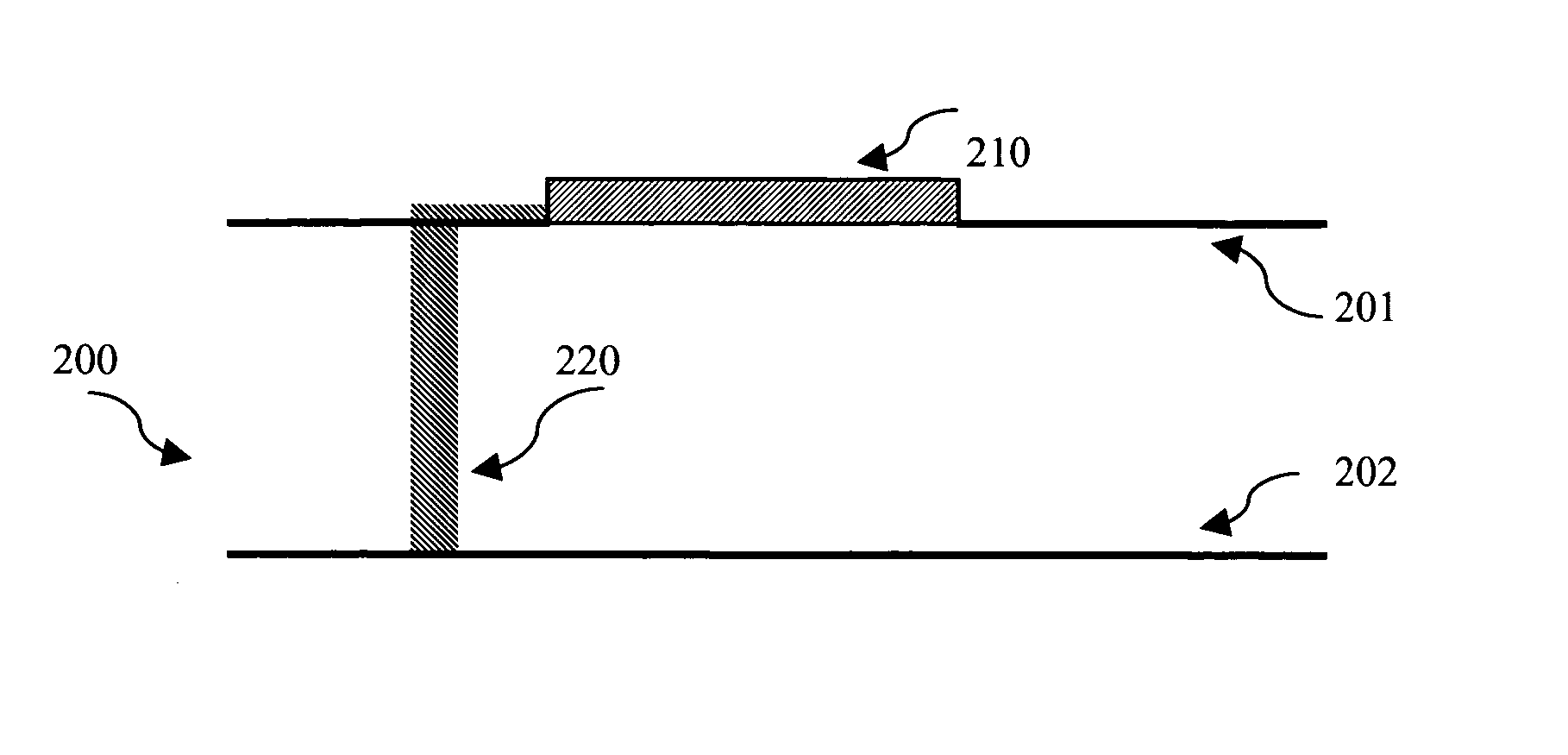
[0012] Using reactive ion etching techniques high aspect ratio features are routinely made with current IC technology. Copper metallization technology includes not only the ability to deposit seed layers but also to deposit the conductor layer and form barrier layers to prevent the diffusion of the copper into the active device regions as well as isolate it electrically from other circuit elements. All metallization schemes require a barrier material between the conductor and the device material to prevent diffusion of the conductor into the active circuit element region with subsequent degradation of circuit performance as well as maintain electrical isolation. Silicon dioxide is the most common barrier material for non-copper based metallization systems; SiO2 has the benefit of providing simultaneously electrical and material isolation. The advent of copper metallization has required extensive research to develop tantalum nitride based and other barrier systems suitable for copper...


PUM


Abstract

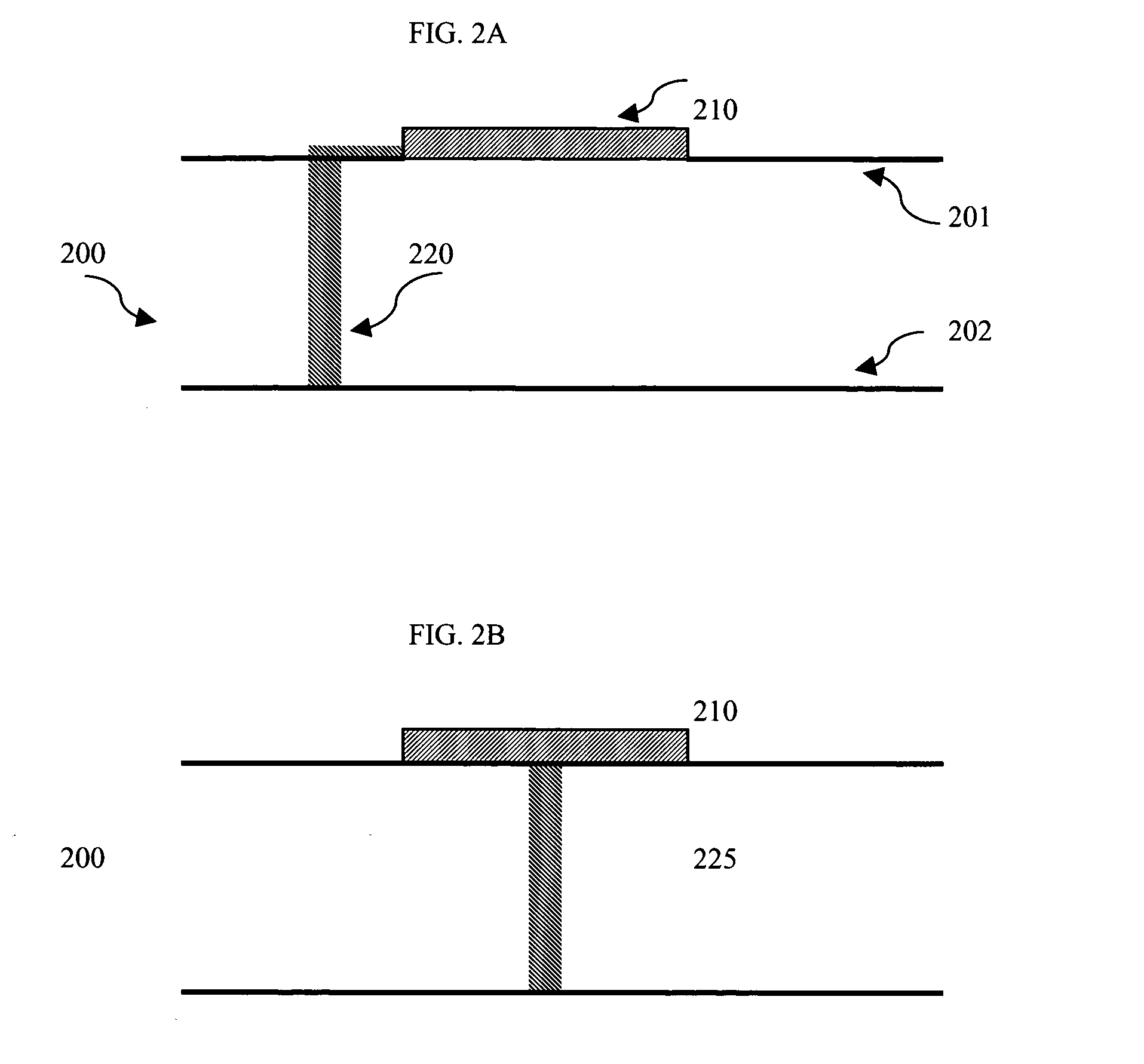
An integrated circuit with conductive channels connecting the bonding pads to alternative surfaces of the IC chip is disclosed. Typically the channels would be formed by reactive ion etching, passivated and then filled with copper or other conductive material. The channels may be formed at alternative points in the wafer processing flow depending on the requirements of the IC. Alternatively the channels may be used for heat sinks; in this case the channel would connect a chip “hot spot” with a conductive package member.

Description

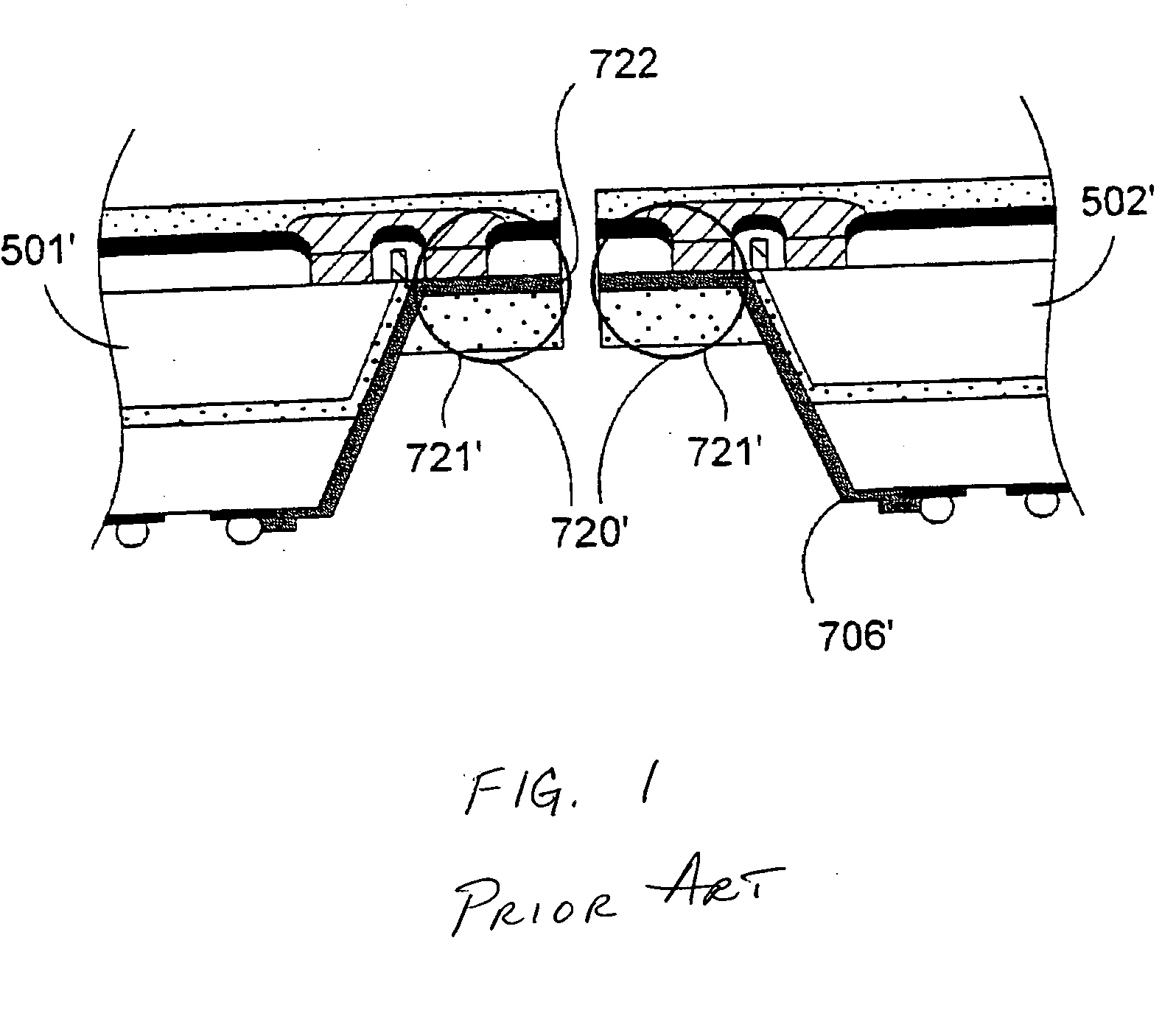
FIELD OF INVENTION [0001] The invention described herein relates generally to semiconductor integrated circuit manufacturing processes. In particular, the invention relates to improved methods of making contact to the bonding pads for side or backside connection. BACKGROUND OF INVENTION [0002] A critical step in the manufacture of all integrated circuit devices is known as “packaging” and involves mechanical and environmental protection of the device chip as well as making electrical interconnection between locations on the silicon chip, known as bonding pads, and external electrical terminals. At present three main technologies are employed for making electrical connections to the integrated circuit: wire bonding, tape automatic bonding (TAB) and flip chip. All three technologies have deficiencies. Chip scale size packages require very small footprints to achieve space improvements. New interconnection techniques are needed to achieve even smaller footprints. [0003] Prior art uses ...

Claims


Application Information

Patent Timeline
IPC IPC(8): H01L21/44H01L21/768H01L23/48
CPCH01L21/76898H01L23/481H01L2924/0002H01L2224/0557H01L2224/05548H01L2224/02372H01L2224/0401H01L2224/04042H01L2224/05552H01L2224/02371
Inventor HARRIS, JAMES M.
Owner HARRIS JAMES M
Learn More