
Nanostructure and nanocomposite based compositions and photovoltaic devices

a technology of nanocomposites and compositions, applied in the field of nanostructures, can solve the problems of marginally better than 10%, low efficiency, and low efficiency of devices, and achieve the effect of improving device efficiency

Inactive Publication Date: 2005-06-16
NANOSYS INC
View PDF46 Cites 215 Cited by
  • Summary
  • Abstract
  • Description
  • Claims
  • Application Information

AI Technical Summary

Benefits of technology

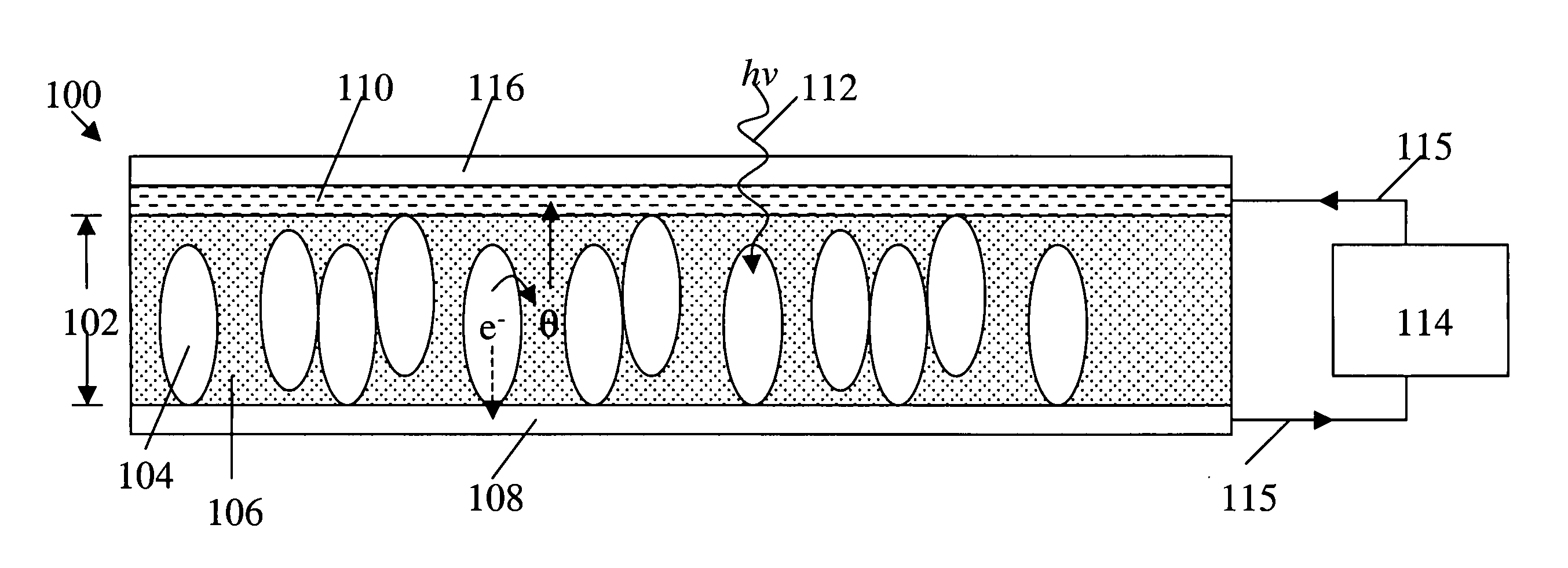
[0019] The overall architecture of the device can be selected based upon the use to which the device is to be put. For example, the overall device can comprise a planar or a non-planar architecture. For example, the device optionally comprises a convex architecture to enhance efficiency of the device in settings where convex architecture is desired. Similarly, in one embodiment, the first electrode layer, the photoactive layer and the second electrode layer are optionally oriented in a coiled architecture, or in a reciprocating stacked architecture.

Problems solved by technology

While these devices are useful in certain applications, their efficiency has been somewhat limited, yielding conversion efficiencies, e.g. solar power to electrical power, of typically marginally better than 10%.
While efficiencies of these devices have been improving through costly improvements to device structure, it is believed that physical limitations on these devices mean they will, at best, achieve a maximum efficiency of around 30%.
For ordinary energy requirements, e.g., public consumption, the relative inefficiency of these devices, combined with their relatively high cost, when compared to other means of energy generation, have combined to inhibit the widespread adoption of solar electricity in the consumer markets.
For example, because of their relative inefficiency, as well as their rigid construction, photovoltaic systems typically require adequate flat space that has appropriate sun exposure at all times, or at least during peak times, to meet the requirements for electricity for which the system is used.

Method used


Image

  • Nanostructure and nanocomposite based compositions and photovoltaic devices
  • Nanostructure and nanocomposite based compositions and photovoltaic devices
  • Nanostructure and nanocomposite based compositions and photovoltaic devices

Examples


example 1

Nanocomposite Photovoltaic Device

[0293] This example describes fabrication of a CdSe nanocrystal-P3HT polymer nanocomposite photovoltaic device. CdSe nanorods have been used; CdSe nanotetrapods can also be used, as can other nanostructure types and / or compositions.

[0294] Substrate Cleaning

[0295] Substrates (e.g., ITO on glass, from Thin Film Devices, Inc., www.tfdinc.com) are cleaned, e.g., using the following procedure. Substrates are wiped with isopropanol, ultrasonicated in isopropanol, ultrasonicated in 2% Hellmanex™ in deionized water, rinsed very thoroughly under flowing deionized water, ultrasonicated in deionized water, ultrasonicated in semiconductor grade acetone, and ultrasonicated in semiconductor grade isopropanol. Each sonication is for 15 minutes. The substrates are then oxygen plasma cleaned, at 200 W (1% reflected power) for 10 minutes with oxygen introduced at a pressure of approximately 400 mTorr into a vacuum of 80 mTorr.

[0296] PEDOT Layer Processing

[0297] P...

example 2

CdSe-CdTe Nanocrystal Photovoltaic Device

[0310] This example describes fabrication of a photovoltaic device comprising two intermixed populations of nanocrystals, CdSe nanocrystals and CdTe nanocrystals.

[0311] Substrate Cleaning

[0312] Substrates (e.g., ITO on glass, from Thin Film Devices, Inc., www.tfdinc.com) are cleaned, e.g., using the following procedure. Substrates are wiped with isopropanol, ultrasonicated in isopropanol, ultrasonicated in 2% Hellmanex™ in deionized water, rinsed very thoroughly under flowing deionized water, ultrasonicated in deionized water, ultrasonicated in semiconductor grade acetone, and ultrasonicated in semiconductor grade isopropanol. Each sonication is for 15 minutes. The substrates are then oxygen plasma cleaned, at 200 W (1% reflected power) for 10 minutes with oxygen introduced at a pressure of approximately 400 mTorr into a vacuum of 80 mTorr.

[0313] PEDOT Layer Processing

[0314] PEDOT / PSS Poly(3,4-ethylenedioxythiophene) poly(styrenesulfonat...

example 3

Doped Polymer and Small Molecule Matrix Nanocomposite Photovoltaic Devices

[0323] This example demonstrates fabrication of nanocomposite photovoltaic devices. The nanocomposite can include, e.g., a polymer matrix, a doped polymer matrix, or a small molecule matrix. As described in the following sections, the example devices include CdSe nanocrystals in a matrix comprising 0-100% P3HT polymer and 100-0% TPD.

[0324] Substrate Cleaning

[0325] Substrates (e.g., ITO on glass, from Thin Film Devices, Inc., www.tfdinc.com) are cleaned, e.g., using the following procedure. Substrates are wiped with isopropanol, ultrasonicated in isopropanol, ultrasonicated in 2% Hellmanex™ in deionized water, rinsed very thoroughly under flowing deionized water, ultrasonicated in deionized water, ultrasonicated in semiconductor grade acetone, and ultrasonicated in semiconductor grade isopropanol. Each sonication is for 15 minutes. The substrates are then oxygen plasma cleaned, at 200 W (1% reflected power) ...


PUM

PropertyMeasurementUnit
Size distributionaaaaaaaaaa
Compositionaaaaaaaaaa
Polarityaaaaaaaaaa

Abstract

Nanocomposite photovoltaic devices are provided that generally include semiconductor nanocrystals as at least a portion of a photoactive layer. Photovoltaic devices and other layered devices that comprise core-shell nanostructures and / or two populations of nanostructures, where the nanostructures are not necessarily part of a nanocomposite, are also provided, as are devices including a recombination material and / or multiple electrodes. Varied architectures for such devices are also provided, including flexible and rigid architectures, planar and non-planar architectures, and the like, as are systems incorporating such devices, and methods and systems for fabricating such devices. Compositions comprising two populations of nanostructures of different materials or nanostructures and a small molecule are also described, as are doped polymer nanocomposites. Compositions useful for making nanocomposites are also described.

Description

CROSS REFERENCE TO RELATED APPLICATIONS [0001] This application is a continuation-in-part of U.S. patent application Ser. No. 10 / 656,802, filed Sep. 4, 2003, entitled “NANOSTRUCTURE AND NANOCOMPOSITE BASED COMPOSITIONS AND PHOTOVOLTAIC DEVICES” by Erik Scher et al., which claims priority to and benefit of U.S. Provisional Patent Application No. 60 / 408,722, filed Sep. 5, 2002, “NANOCOMPOSITES” by Mihai Buretea et al., U.S. Provisional Patent Application No. 60 / 421,353, filed Oct. 25, 2002, “NANOCOMPOSITE BASED PHOTOVOLTAIC DEVICES” by Erik Scher et al., and U.S. Provisional Patent Application No. 60 / 452,038, filed Mar. 4, 2003, “NANOCOMPOSITE BASED PHOTOVOLTAIC DEVICES” by Erik Scher et al., each of which is incorporated herein by reference in its entirety for all purposes.STATEMENT AS TO RIGHTS TO INVENTIONS MADE UNDER FEDERALLY SPONSORED RESEARCH AND DEVELOPMENT [0002] Portions of this invention may have been made with United States Government support under National Reconnaissance ...

Claims


Application Information

Patent Timeline
IPC IPC(8): H01L31/00H01L31/0264H01L31/036H01L31/04
CPCB82Y10/00B82Y20/00B82Y30/00H01L27/302H01L29/0665H01L29/0673Y02E10/549H01L31/0352H01L51/0036H01L51/0037H01L51/4213H01L51/426H01L51/4266H01L29/127Y02P70/50H10K30/57H10K85/1135H10K85/113H10K30/352H10K30/10H10K30/50H10K30/35
Inventor SCHER, ERIK C.BURETEA, MIHAI A.CHOW, CALVINEMPEDOCLES, STEPHENMEISEL, ANDREASPARCE, J. WALLACEWHITEFORD, JEFF
Owner NANOSYS INC
Learn More