Micro/nano-fabricated glucose sensors using single-walled carbon nanotubes
a carbon nanotube and glucose sensor technology, applied in specific use bioreactors/fermenters, enzyme production/based bioreactors, biomass after-treatment, etc., to achieve good effects
- Summary
- Abstract
- Description
- Claims
- Application Information
AI Technical Summary
Benefits of technology
Problems solved by technology
Method used
Image
Examples
example 1
[0032] It is known in the art that approximately 70% of grown SWCNTs have semiconducting characteristics, while the remaining approximate 30% have metallic characteristics. [R. Krupke, F. Henmich, H. v. Lohneysen, and M. M. Kappes, “Separation of Metallic from Semiconducting Single-Walled Carbon Nanotubes,”Science, vol. 301, pp. 344-347, 2003.] According to the mechanism mentioned previously, however, the present invention comprises sufficient metallic SWCNTs in a nanotube population having a grouped or bundled configuration to effectively sense hydrogen. Dielectrophoresis can be used to collect SWCNTs with similar electrical (e.g., metallic) properties. As demonstrated below, a non-uniform electric field between a pair of electrodes induces an attractive dielectrophoretic forces on particles, e.g., SWCNTs, suspended in a suitable medium (e.g., dichlorobenzene solution). By the dielectrophoretic force at a specific frequency band (e.g., at 1 MHz), metallic SWCNTs can be selectively ...
example 2
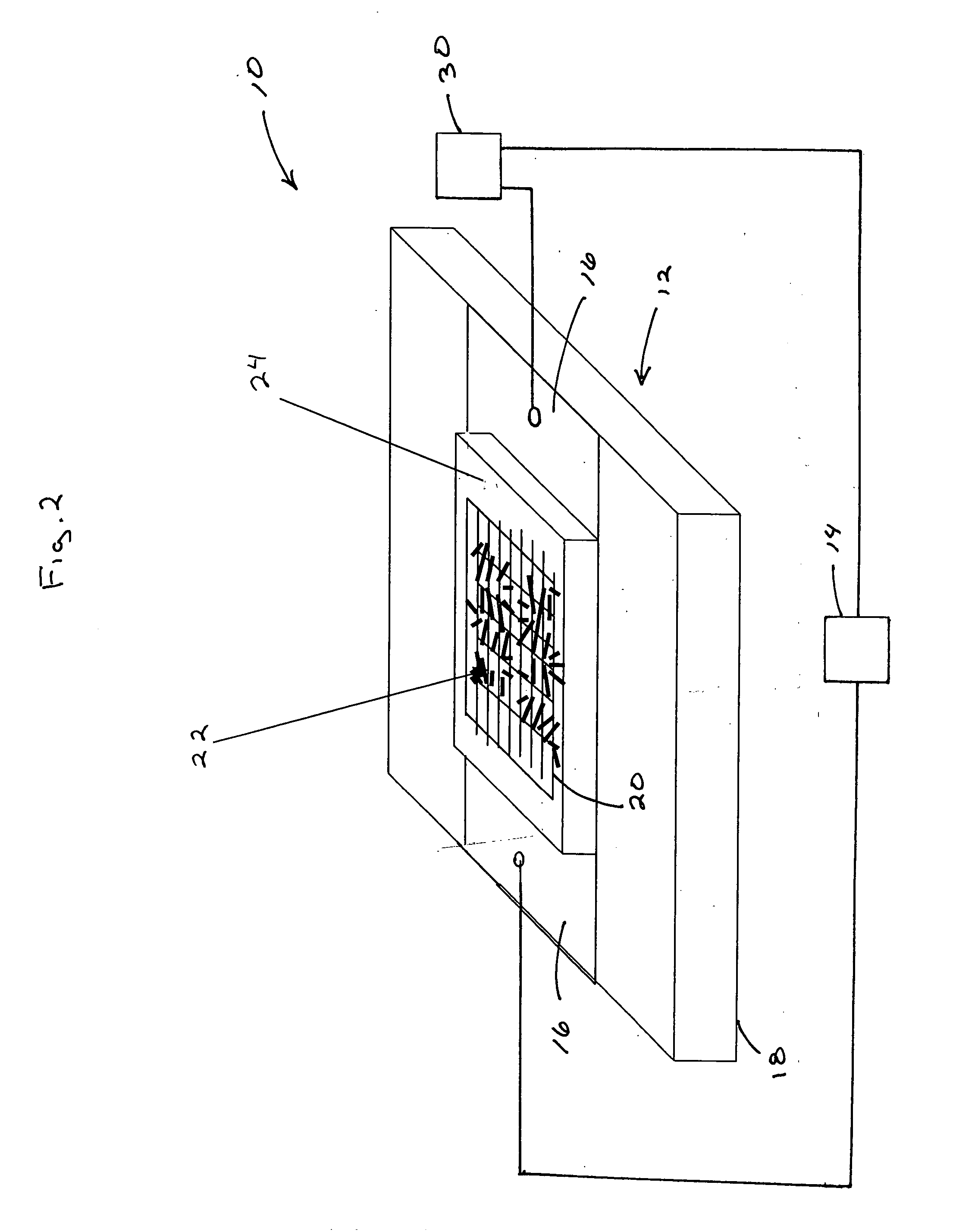
[0033] As mentioned above, FIGS. 2-4 show schematically the fabrication and structure of a glucose sensor and / or apparatus in accordance with this invention. Further details relating to substrate preparation and oxidation, electrode deposition and patterning, and corresponding lithographic techniques are provided in co-pending application Ser. No. 10 / 426,925, in particular Examples 16-17 and FIGS. 20, 23-26 thereof, filed Apr. 30, 2003, the entirety of which is incorporated herein by reference. Likewise, as would be understood by those skilled in the art, information relating to substrate, electrode and circuit preparation is also provided in the aforementioned and incorporated '020 patent, in particular columns 3-6 and by way of the figures referenced therein. More specifically, with reference to FIG. 5, SWCNTs (commercially, from HiPCo) individually separated and dispersed in 1,2-dichlorobenzene by sonication (38) were deposited on an oxidized Si substrate (32), as described above...
example 3
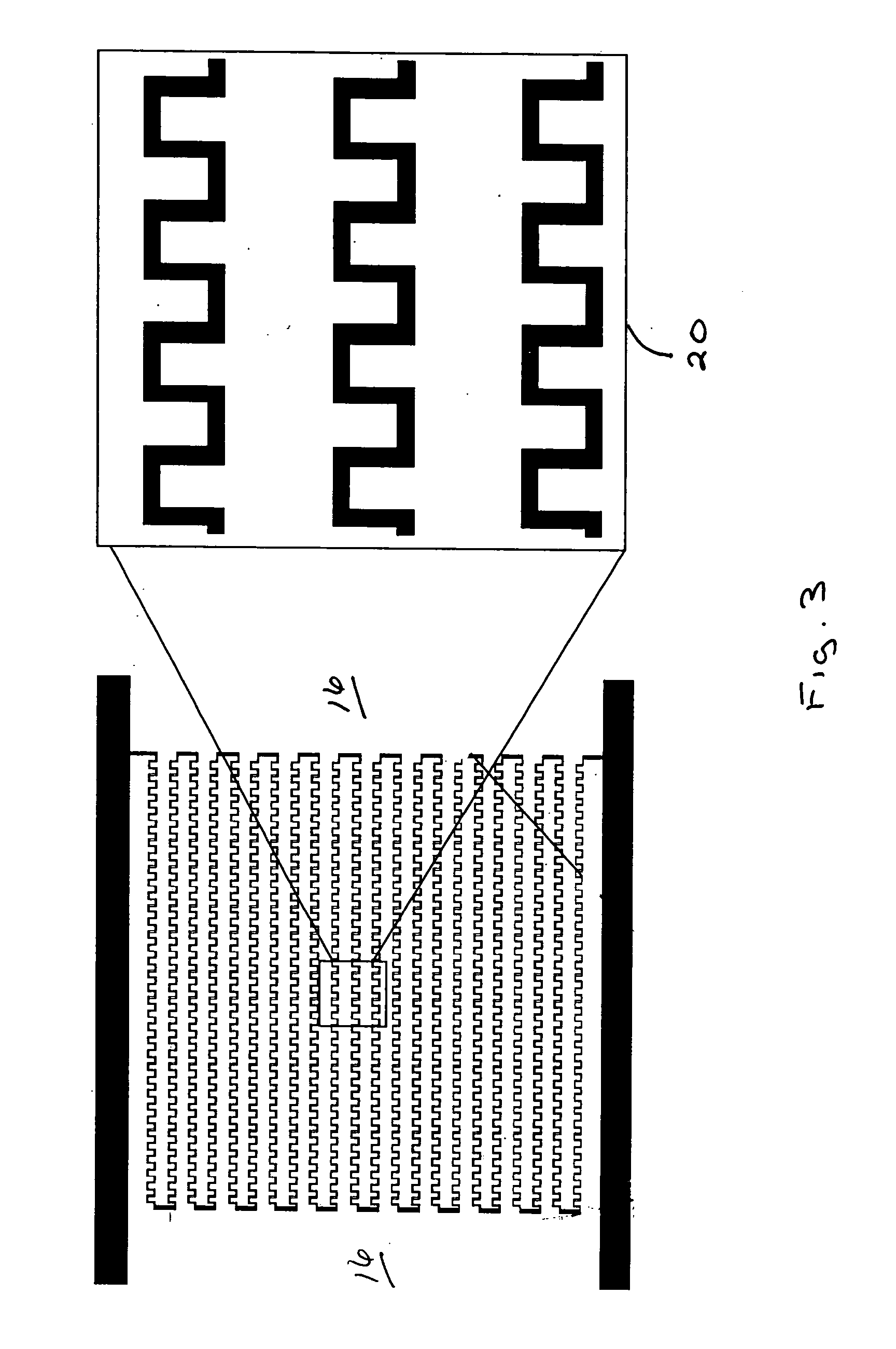
[0034] Even though the deposited SWCNTs were barely visible under scanning electron microscopy (SEM), the deposition result was confirmed by a finite resistance after deposition. The electrodes in FIG. 3 were designed and fabricated to have an interdigitated comb (i.e., a so-called “Ramen”) structure for a higher electric field gradient and maximum concentration of deposited SWCNTs. As expected, dielectrophoresis aggregated SWCNTs around the electrodes, due to a concentrated electric field. The deposited SWCNTs and porous structure of the GOD-immobilized hydrogel matrix can be observed via SEM.
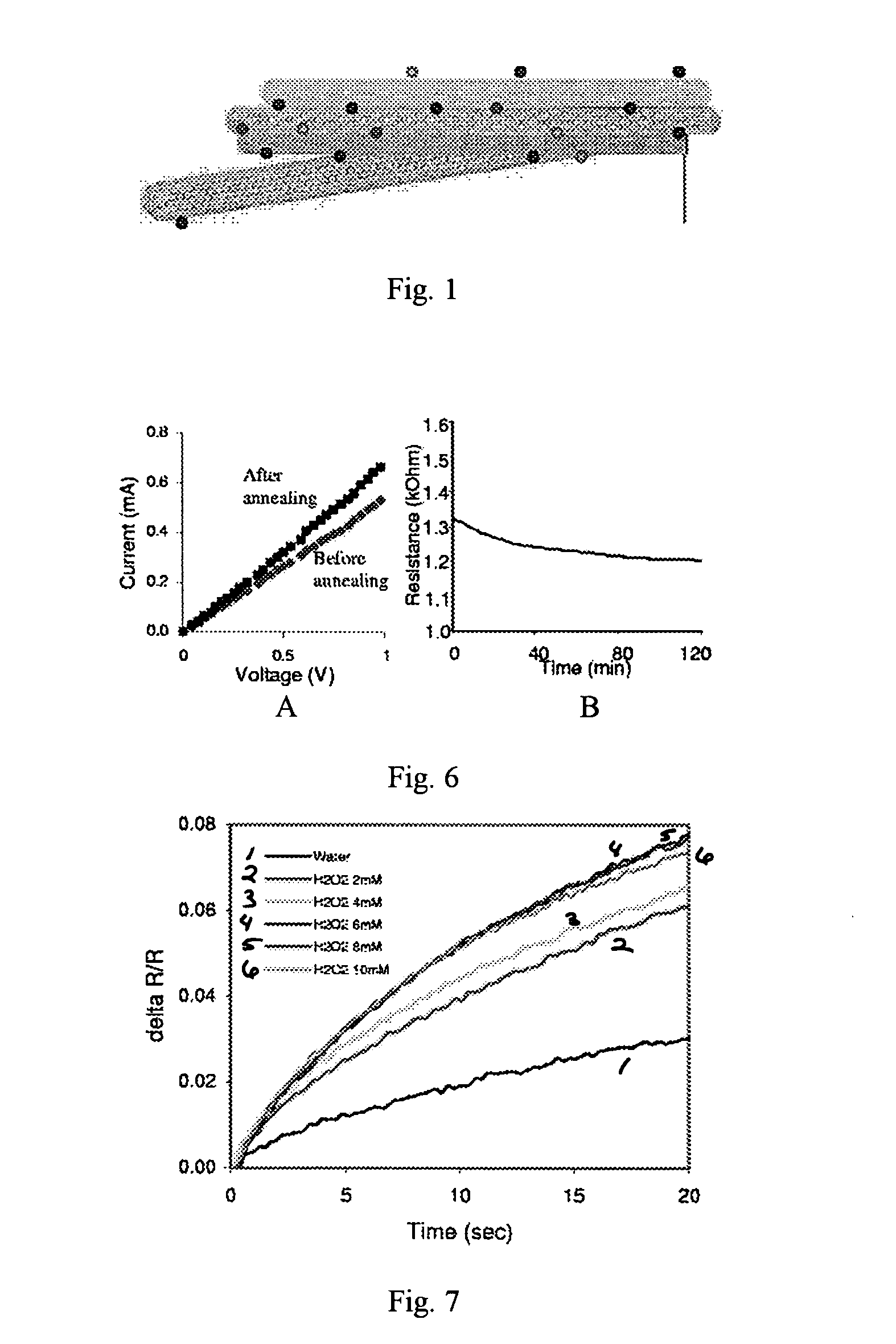
[0035] When a resistance was measured right after the SWCNT deposition, the value was approximately ˜2 kOhm. When the solvent was completely evaporated, a better electrical contact was made, and the resistance reduced to a half, ˜1 kOhm. It was confirmed that the deposited SWCNTs have metallic characteristics as shown in FIG. 6A. During the measurement, the resistance decreased due to a sligh...
PUM
| Property | Measurement | Unit |
|---|---|---|
| volume | aaaaa | aaaaa |
| current | aaaaa | aaaaa |
| volumes | aaaaa | aaaaa |
Abstract
Description
Claims
Application Information
 - R&D
- Intellectual Property
- Life Sciences
- Materials
- Tech Scout
- Unparalleled Data Quality
- Higher Quality Content
- 60% Fewer Hallucinations
Browse by: Latest US Patents, China's latest patents, Technical Efficacy Thesaurus, Application Domain, Technology Topic, Popular Technical Reports.
© 2025 PatSnap. All rights reserved.Legal|Privacy policy|Modern Slavery Act Transparency Statement|Sitemap|About US| Contact US: help@patsnap.com


