Methods for machine detection of al least one aspect of an object, methods for machine identification of a person, and methods of forming electronic systems

a technology of machine detection and object, applied in the field of electronic systems, can solve the problems of limited performance of tfts, limited carrier mobilities, and high power consumption

Inactive Publication Date: 2005-05-12
ROUND ROCK RES LLC
View PDF3 Cites 58 Cited by
  • Summary
  • Abstract
  • Description
  • Claims
  • Application Information

AI Technical Summary

Problems solved by technology

A problem associated with conventional TFT constructions is that grain boundaries and defects can limit carrier mobilities.
High voltage (and therefore high power consumption), and large areas are utilized for the TFTs, and the TFTs exhibit limited performance.
TFTs thus have limited commercial application and currently are utilized primarily for large area electronics.
Performance enhancements of standard field effect transistor devices are becoming limited with progressive lithographic scaling in conventional applications.
Although various techniques have been developed for substantially controlling nucleation and grain growth processes of semiconductor materials, grain orientation control is lacking.
Further, the post-anneal treatment utilized in conjunction with MILC can be unsuitable in applications in which a low thermal budget is desired.

Method used


Image

  • Methods for machine detection of al least one aspect of an object, methods for machine identification of a person, and methods of forming electronic systems
  • Methods for machine detection of al least one aspect of an object, methods for machine identification of a person, and methods of forming electronic systems
  • Methods for machine detection of al least one aspect of an object, methods for machine identification of a person, and methods of forming electronic systems

Examples


Embodiment Construction

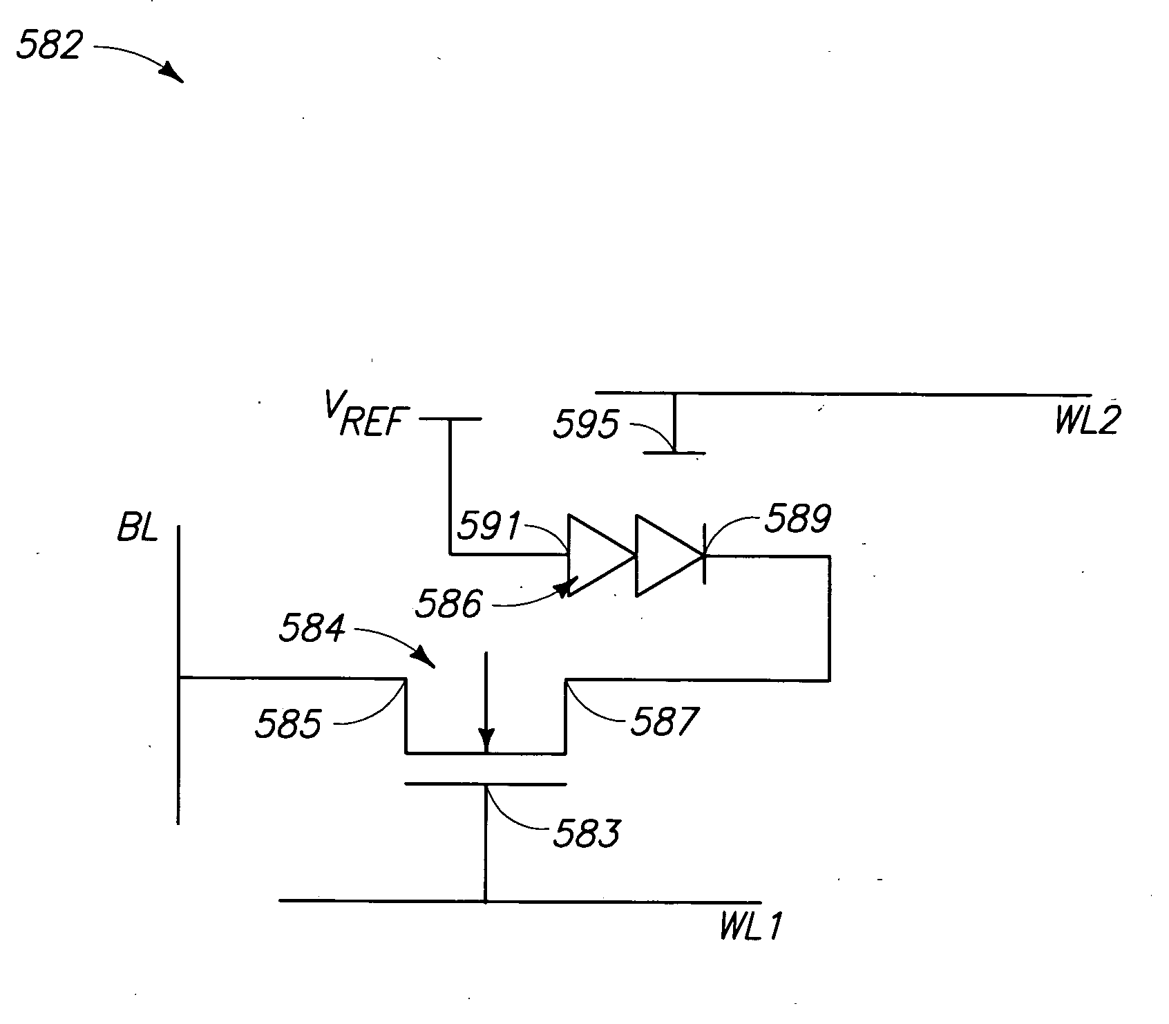
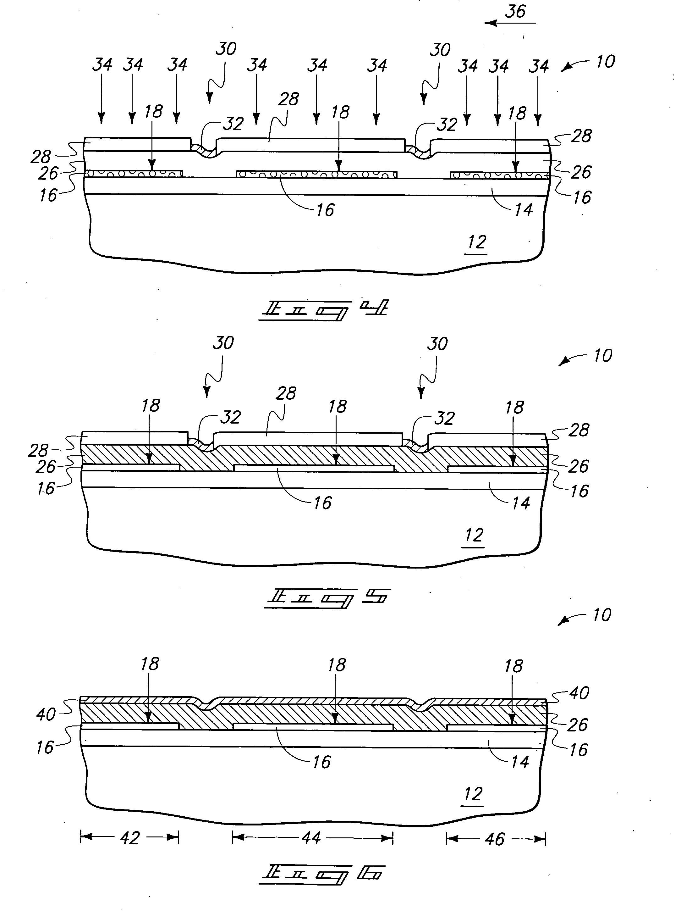
[0059] The invention pertains to various data storage devices, logic devices, and electronic systems comprising data storage devices and logic devices. Prior to the discussion of the exemplary data storage devices, logic devices and electronic systems, a processing sequence for forming and utilizing preferred Si / Ge materials is described with reference to FIGS. 1-9.

[0060] Referring to FIG. 1, a fragment of a semiconductor construction 10 is illustrated at a preliminary processing stage. To aid in interpretation of the claims that follow, the terms “semiconductive substrate” and “semiconductor substrate” are defined to mean any construction comprising semiconductive material, including, but not limited to, bulk semiconductive materials such as a semiconductive wafer (either alone or in assemblies comprising other materials thereon), and semiconductive material layers (either alone or in assemblies comprising other materials). The term “substrate” refers to any supporting structure, ...


PUM


Abstract

The invention includes electronic systems comprising Si / Ge substrates. The electronic systems can include data storage devices and / or logic devices having active regions extending into a crystalline Si / Ge material. An entirety of the portion of an active region within the crystalline Si / Ge material can be within a single crystal of the material. The assemblies can be utilized for detecting properties of objects, and in particular aspects can be incorporated into assemblies utilized for identifying persons. The assemblies can be fabricated over a range of versatile substrates, including, for example, glass, alumina or metal.

Description

TECHNICAL FIELD [0001] The invention pertains to electronic systems. In particular aspects, the invention pertains to constructions for detecting at least one property of an object, and in further aspects the invention pertains to assemblies for identifying persons. BACKGROUND OF THE INVENTION [0002] SOI technology differs from traditional bulk semiconductor technologies in that the active semiconductor material of SOI technologies is typically much thinner than that utilized in bulk technologies. The active semiconductor material of SOI technologies will typically be formed as a thin film over an insulating material (typically oxide), with exemplary thicknesses of the semiconductor film being less than or equal to 2000 Å. In contrast, bulk semiconductor material will typically have a thickness of at least about 200 microns. The thin semiconductor of SOI technology can allow higher performance and lower power consumption to be achieved in integrated circuits than can be achieved wit...

Claims


Application Information

Patent Timeline
Patent Type & Authority Applications(United States)
IPC IPC(8): H01L21/28H01L21/336H01L27/06H01L27/108H01L27/12H01L29/423H01L29/51H01L29/786H01L29/788
CPCH01L21/28194H01L27/0688H01L27/10817H01L27/1203H01L29/42324H01L29/513H01L29/7881H01L29/518H01L29/66742H01L29/66825H01L29/7842H01L29/78687H01L29/78696H01L29/517H10B12/318
Inventor BHATTACHARYYA, ARUP
Owner ROUND ROCK RES LLC
Why Eureka
Try Eureka