
Method of production of multilayer ceramic electronic device

Active Publication Date: 2005-05-05
TDK CORPARATION
View PDF2 Cites 22 Cited by
  • Summary
  • Abstract
  • Description
  • Claims
  • Application Information

AI Technical Summary

Benefits of technology

[0010] An object of the present invention is to provide a method of production of a multilayer ceramic capacitor or other multilayer ceramic electronic device with few structural defects and improved highly accelerated life test value.
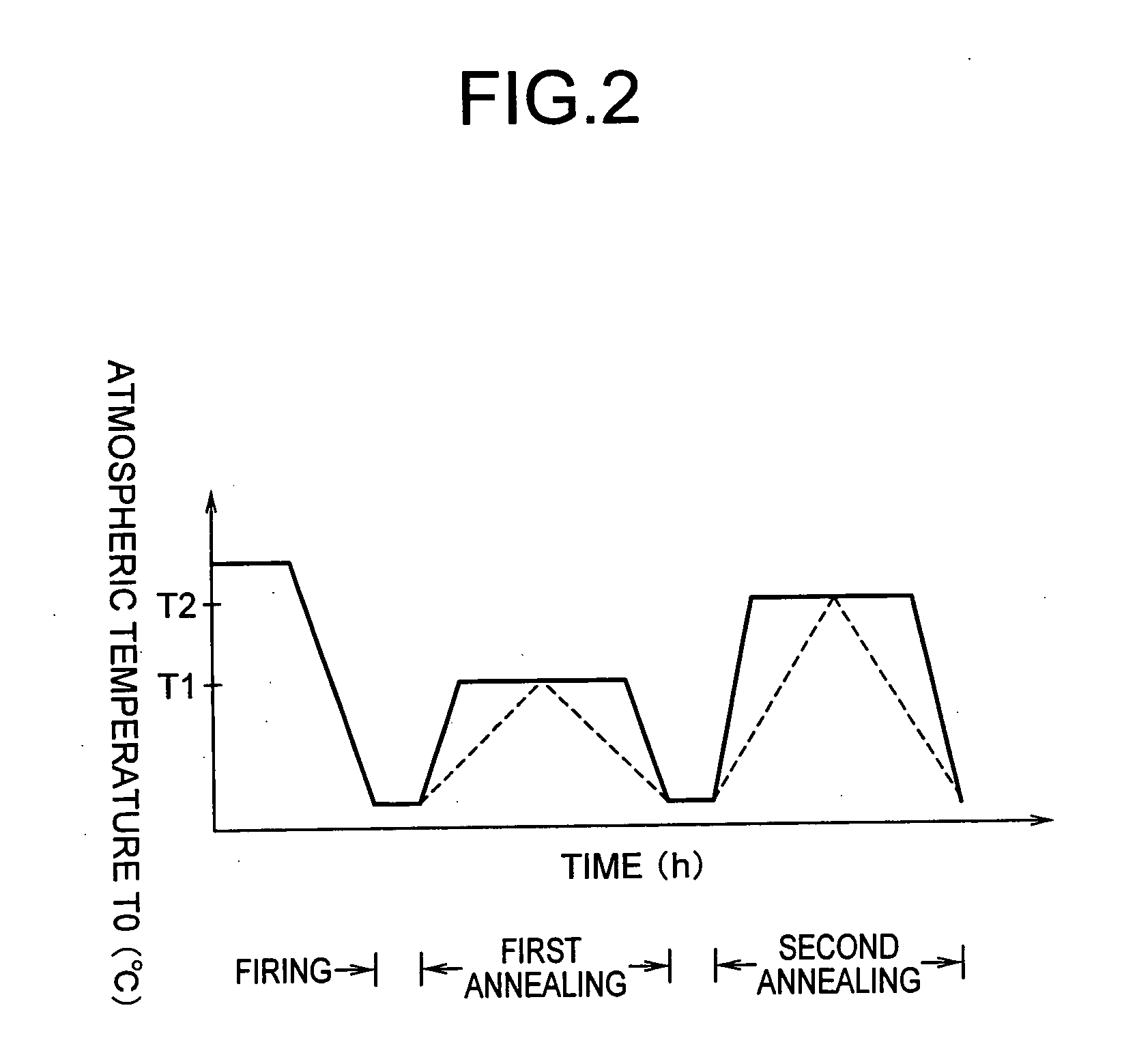
[0011] The inventors discovered that by performing annealing after firing step by step a plurality of times, the object of the present invention can be achieved and thereby completed the present invention.
[0023] According to the present invention, as the means for optimizing the annealing conditions, annealing is performed stepwise a plurality of times. Due to this, the poor conduction and other structural defects due to segregation and precipitation of Mn which had occurred in the past at the vicinity and ends of the internal electrode layers are suppressed. As a result, there is also no longer any disconnects of the internal electrode layers due to these structural defects and the coverage-rate of the internal electrode layers is raised and contributes to an improvement of the capacity (or prevention of a drop).
[0024] Further, the insulation resistance and accelerated life (highly accelerated life test value) of the obtained multilayer ceramic capacitor or other multilayer ceramic electronic device are improved.

Problems solved by technology

In the past, when adding Mn to the dielectric layers, the sintered body obtained by firing a green chip containing the dielectric layers had to be suitably annealed or else MnO would segregate (precipitate) in the vicinity or at the ends of the internal electrode layers—resulting in problems such as structural defects or disconnects of internal electrode layers.
That is, if annealing was not suitably performed, it became a cause of a drop in the yield, reliability, etc. of the capacitors.
However, with a single annealing, if the holding temperature is too low, there is a tendency for the reoxidation of the dielectric layers to become insufficient, the insulation resistance to deteriorate, and the accelerated life (highly accelerated life test value) to also become shorter.
Conversely, if the holding temperature is too high, the reoxidation of the dielectric layers is performed well, but even the internal electrode layers end up being oxidized and therefore not only does the capacity fall, but also there is tendency for the dielectric base material to end up being reacted with and the capacity-temperature characteristic, insulation resistance, and accelerated life to deteriorate.
That is, with just a single annealing, optimization of the stabilization (holding) temperature and time was difficult.

Method used

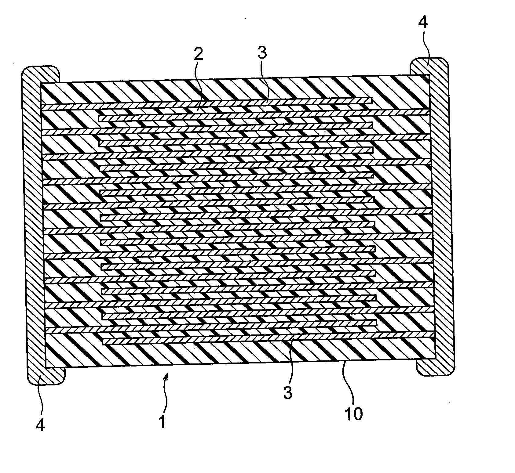
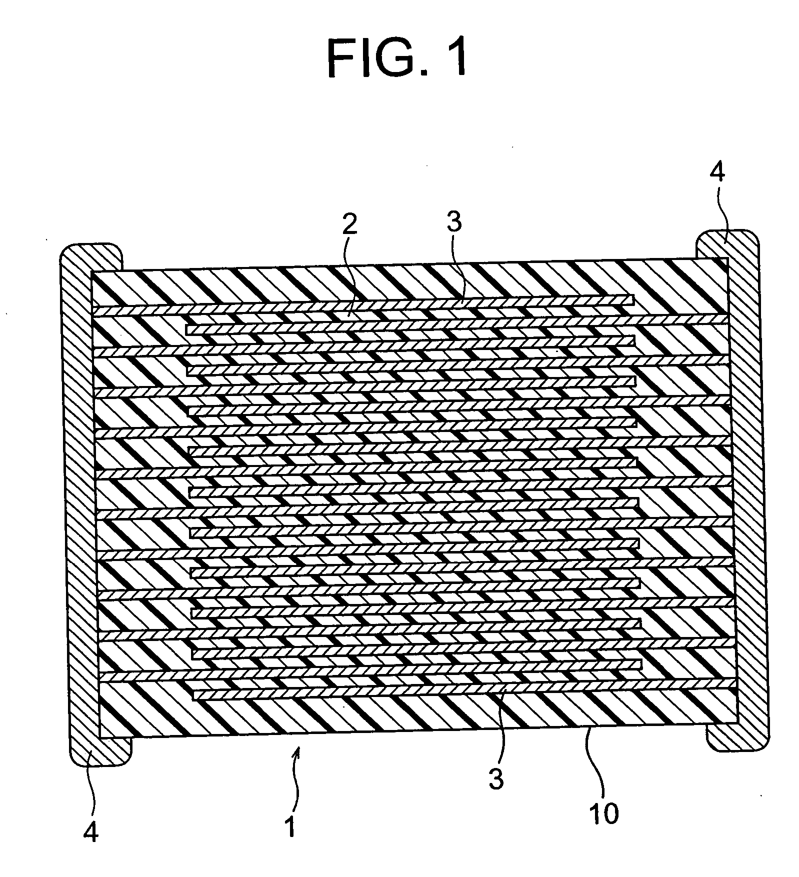

Image

  • Method of production of multilayer ceramic electronic device
  • Method of production of multilayer ceramic electronic device
  • Method of production of multilayer ceramic electronic device

Examples


examples

[0080] Next, the present invention will be explained in more detail by giving examples further specifying the embodiments of the present invention. However, the present invention is not limited to just these embodiments.

[0081] The routine shown below was used to prepare samples of multilayer ceramic capacitors.

[0082] Preparation of Pastes

[0083] First, the dielectric layer paste was prepared as follows:

[0084] As the starting materials for preparing the dielectric material, main ingredient materials (SrCO3, CaCO3, TiO2, and ZrO2) and secondary ingredient materials (V2O5, Al2O3, MnCO3, BaCO3, CaCO3, SiO2, etc.) having average particle sizes of 0.1 to 1 μm were prepared.

[0085] Next, the main ingredient materials and the secondary ingredient materials were weighed and mixed so that the compositions after firing had the following ratios of composition and then dried to obtain the dielectric materials.

[0086] In Samples 1 to 3, they were mixed to give 100 moles of {(Ca0.6Sr0.4)O}.(Zr0...


PUM

PropertyMeasurementUnit
Partial pressureaaaaaaaaaa
Temperatureaaaaaaaaaa

Abstract

A method of production of a multilayer ceramic capacitor or other multilayer ceramic electronic device with few structural defects and improved highly accelerated life, that is, a method of production of a multilayer ceramic electronic device having a firing step of firing a stack comprised of a dielectric layer paste and an internal electrode layer paste including a base metal alternately arranged in a plurality of layers, a first annealing step of annealing, at a temperature T1 of 600 to 900° C., the stack after firing and a second annealing step of annealing, at a temperature T2 of 900 to 1200° C. (however, excluding 900° C.), the stack after said first annealing.

Description

BACKGROUND OF THE INVENTION [0001] 1. Field of the Invention [0002] The present invention relates to a method of production of a multilayer ceramic capacitor or other multilayer ceramic electronic device. [0003] 2. Description of the Related Art [0004] In recent years, as the material for internal electrode layers used in a multilayer ceramic capacitor, a typical example of a multilayer ceramic electronic device, it has become possible to use nickel and other inexpensive base metals instead of platinum, palladium, and other expensive precious metals. Major reductions in cost have been realized. [0005] However, for suitable metallization of internal electrode layers using base metals, the green chip has to be fired in a reducing atmosphere. To give the dielectric materials resistance to reduction in firing in a reducing atmosphere, sometimes Mn is added to the dielectric layers contained in the green chips. Further, to enable reoxidation of the dielectric layers in the sintered body ...

Claims


Application Information

Patent Timeline
IPC IPC(8): H01G4/12C04B35/49H01G4/30H01G13/00H01L21/44
CPCC04B35/465H01G4/30C04B35/486C04B35/49C04B35/6262C04B35/6264C04B35/638C04B2235/3203C04B2235/3206C04B2235/3208C04B2235/3213C04B2235/3215C04B2235/3217C04B2235/3224C04B2235/3225C04B2235/3239C04B2235/3244C04B2235/3251C04B2235/3256C04B2235/3258C04B2235/3262C04B2235/3409C04B2235/3418C04B2235/3436C04B2235/3454C04B2235/5445C04B2235/652C04B2235/6562C04B2235/6565C04B2235/6567C04B2235/6582C04B2235/6584C04B2235/6588C04B2235/662C04B2235/663C04B2235/79H01G4/12C04B35/47
Inventor WATANABE, YASUOENDOH, KENTATAKAHARA, WATARU
Owner TDK CORPARATION
Learn More