Ripple converter
a converter and converter technology, applied in the field of ripple converters, can solve the problems of difficult to predict the characteristics of the capacitor attached to the module, the driving frequency cannot be set to a desired value, and the description is not necessarily accurate, so as to achieve the effect of maintaining stable oscillation
- Summary
- Abstract
- Description
- Claims
- Application Information
AI Technical Summary
Benefits of technology
Problems solved by technology
Method used
Image
Examples
first preferred embodiment
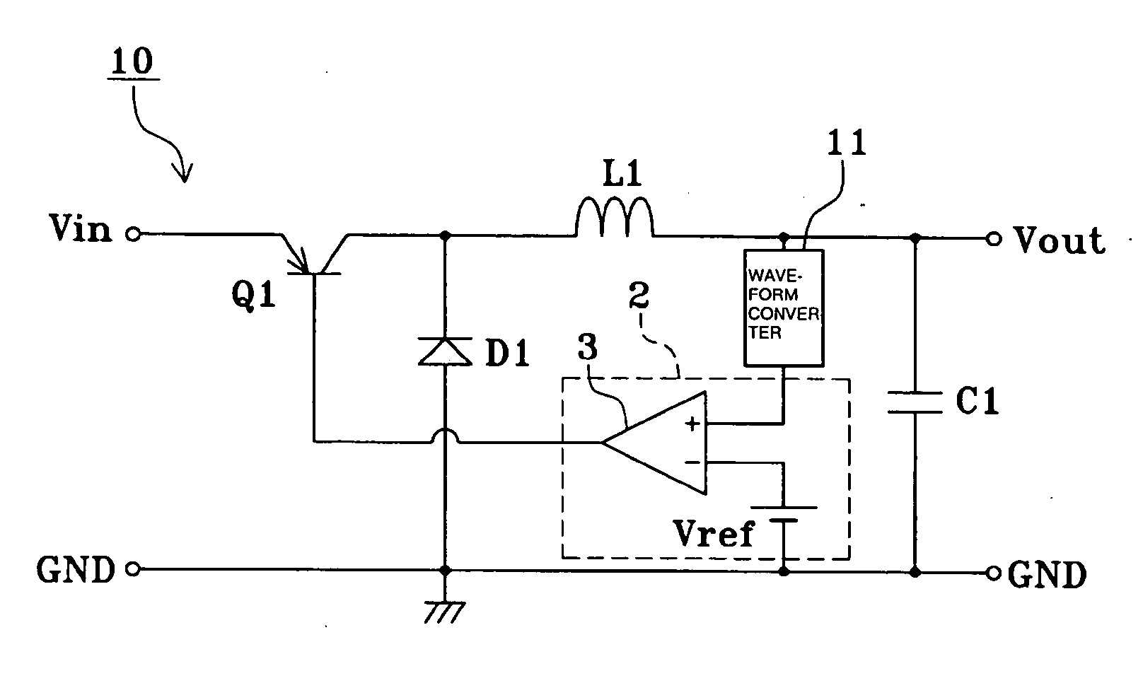
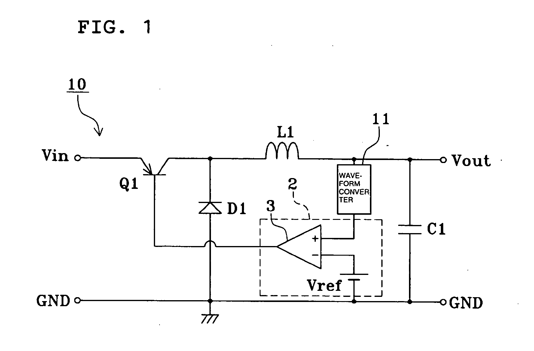
[0038]FIG. 1 shows a circuit diagram of a ripple converter according to a preferred embodiment of the present invention. In FIG. 1, elements corresponding or equivalent to those in FIG. 14B are designated by the same numerals, and descriptions thereof will be omitted.
[0039] In a ripple converter 10 shown in FIG. 1, a waveform converter 11 is disposed on a connecting path between the output terminal Vout and the non-inverting input terminal of the comparator 3. The ripple converter 10 is otherwise the same as the ripple converter 1 according to the related art shown in FIG. 14. In the ripple converter 10, the waveform converter 11 and the comparing unit 2 define a control circuit for exercising feedback control of the ON / OFF of a switching element according to ripple in an output voltage.
[0040] In the ripple converter 10, the waveform of the output voltage vo is converted by the waveform converter 11, and a result of the waveform conversion is compared with the reference voltage vr...
second preferred embodiment
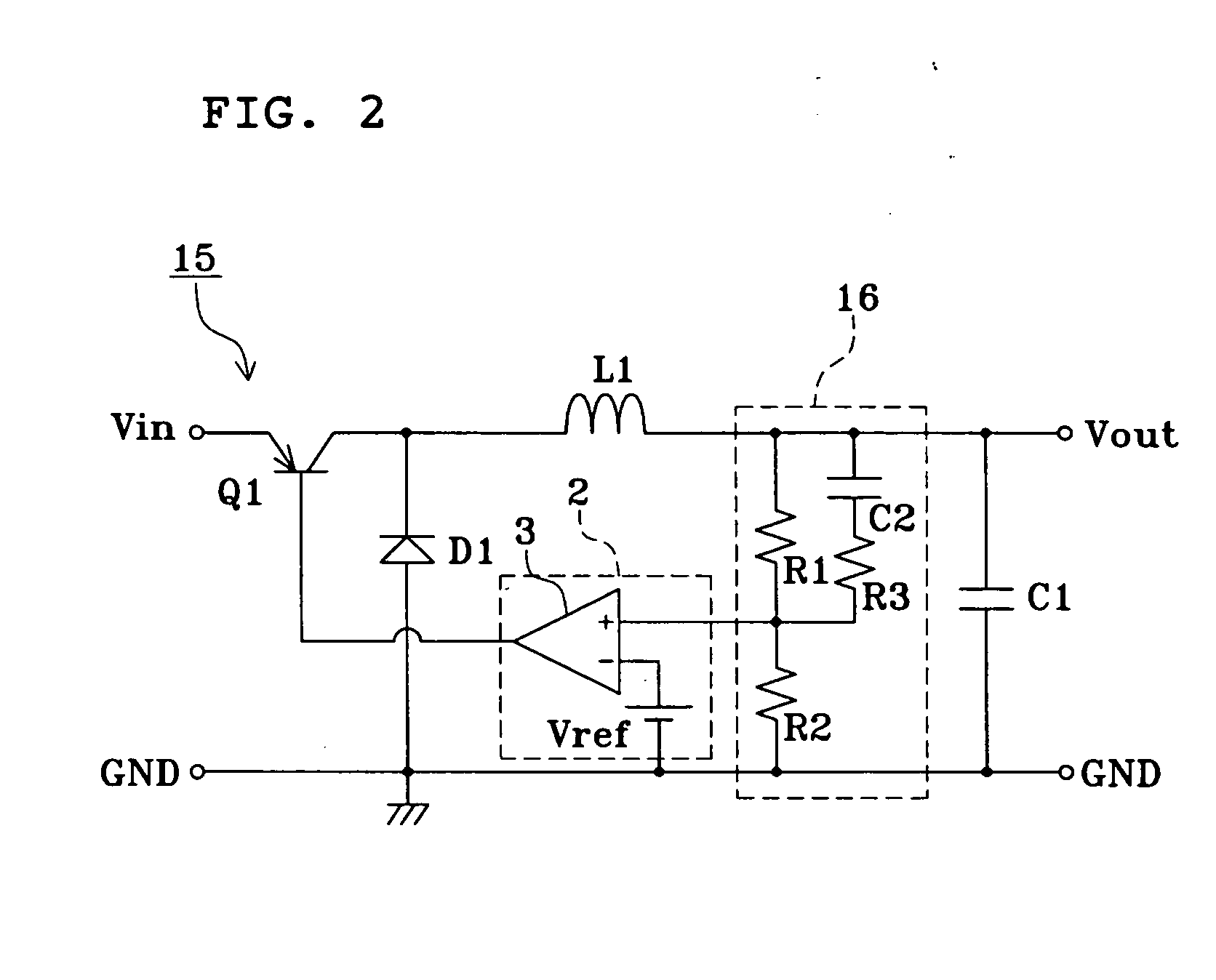
[0041]FIG. 2 shows a circuit diagram of a ripple converter according to another preferred embodiment of the present invention. In FIG. 2, elements corresponding to those in FIG. 1 are designated by the same numerals, and descriptions thereof will be omitted.
[0042] In a ripple converter 15 shown in FIG. 2, the output terminal Vout is connected to the ground via resistors R1 and R2 in series. Furthermore, a capacitor C2 and a resistor R3, connected in series with each other, are connected in parallel to the resistor R1. A node between the resistors R1 and R2 is connected to the non-inverting input terminal of the comparator 3. That is, the resistors R1, R2, and R3, and the capacitor C2 define a waveform converter 16.
[0043] Of the elements of the waveform converter 16, the resistors R1 and R2 provide a circuit for inputting a voltage ver1 that is proportional to the output voltage vo to the non-inverting input terminal of the comparator 3. The capacitor C2 and the resistors R3 and R2...
third preferred embodiment
[0048]FIG. 5 shows a circuit diagram of a ripple converter according to yet another preferred embodiment of the present invention. In FIG. 5, elements corresponding to those in FIG. 2 are designated by the same numerals, and descriptions thereof will be omitted.
[0049] In a ripple converter 18 shown in FIG. 5, instead of the capacitor C2 and the resistor R3 in FIG. 2, a resistor R4 and a capacitor C3, connected in series with each other, are connected in parallel to the resistor R2. Thus, the resistors R1, R2, and R4, and the capacitor C3 define a waveform converter 19.
[0050] Of the elements of the waveform converter 19, the resistors R1 and R2 provide a circuit for inputting a value ver1 that is proportional to the output voltage vo to the non-inverting input terminal of the comparator 3. The resistors R1 and R4 and the capacitor C3 provide a circuit (integrator) for inputting a value ver2 obtained by integrating the output voltage vo to the non-inverting input terminal of the com...
PUM
 Abstract
Description
Claims
Application Information
 - R&D
- Intellectual Property
- Life Sciences
- Materials
- Tech Scout
- Unparalleled Data Quality
- Higher Quality Content
- 60% Fewer Hallucinations
Browse by: Latest US Patents, China's latest patents, Technical Efficacy Thesaurus, Application Domain, Technology Topic, Popular Technical Reports.
© 2025 PatSnap. All rights reserved.Legal|Privacy policy|Modern Slavery Act Transparency Statement|Sitemap|About US| Contact US: help@patsnap.com


