
Method and apparatus for network with multilayer metalization

a multi-layer metalization and network technology, applied in data switching networks, data switching networks, architectures with multiple processing units, etc., can solve the problems of not being able to evenly spread wires across all channels without increasing channel widths, superlinear growth of switching requirements with an increase in the number of compute blocks, and hierarchical scheme not eliminating asymptotic switch requirements. , to achieve the effect of fast and guaranteed routing

Inactive Publication Date: 2005-03-24
CALIFORNIA INST OF TECH
View PDF31 Cites 33 Cited by
  • Summary
  • Abstract
  • Description
  • Claims
  • Application Information

AI Technical Summary

Benefits of technology

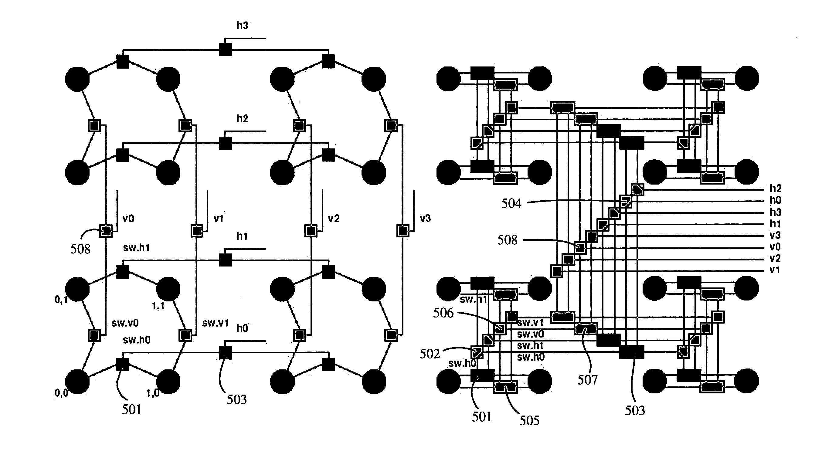
Some embodiments according to the present invention support mapping a BFT / HSRA topology to a MoT topology, which allows for an improved BFT / HSRA layout. Further, using this mapping and the layout according to embodiments of the present invention, a BFT / HSRA topology can be used to layout any graph.
Some embodiments according to the present invention may provide better scalability than the flat, Manhattan interconnect topology described above. Assuming the number of base channels, C, remains constant for increasing design size, the total number of switches per LUT in embodiments according to the present invention generally converges to a constant [O(1)] independent of design size. As discussed above, the flat, Manhattan interconnect generally requires O(Np−0.5) switches per LUT. Given sufficient wiring layers, embodiments of the present invention can maintain a constant area per logic block as the design scales up. Asymptotically, the number of switches in any path in embodiments of the present invention needs to only grow as O(log(N)). Analysis of designs using embodiments according to the present invention shows small C values that do not grow with design size, and total switch requirements that are 26% smaller than those achieved using the flat, Manhattan interconnect topology.
Other embodiments according to the present invention provide a method for fast, guaranteed routing. Such embodiments generally comprise recursively bisecting a network, mapping the bisected network to a BFT topology, and then populating the mapped network using the efficient layout disclosed herein and randomly adding shortcuts, corner turns, and additional uplinks. The network parameters can be selected such that no back tracking is needed in the mapping and the placement and routing will be successful.

Problems solved by technology

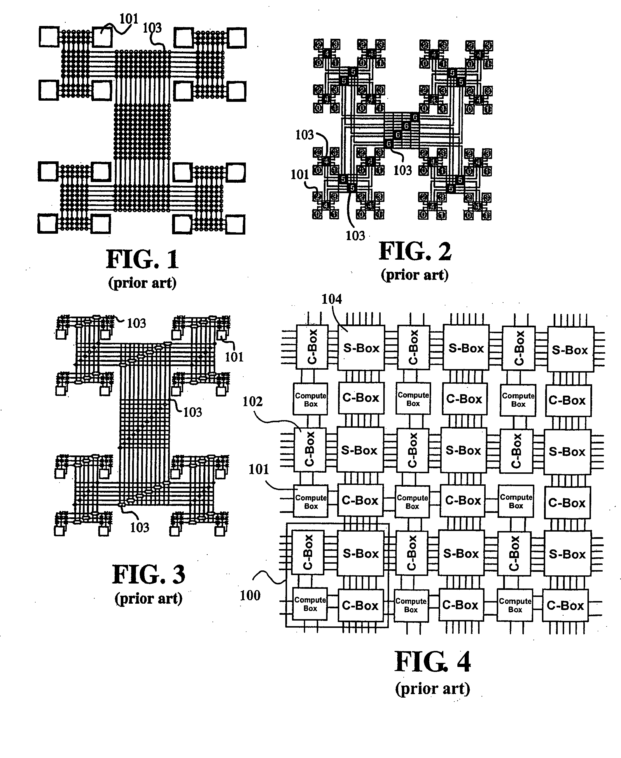
However, the mesh will generally require more wire channels than this because: 1) the calculation is based only on bisection wires, but the channels may need to be wider to hold wires in some of the recursive cuts; and 2) the calculation assumes optimal wire spreading, but it may not be possible to spread wires evenly across all channels without increasing channel widths in the orthogonal channels.
However, such fixed segmentation schemes usually only change the constants related to the number of switches require and generally do not change the asymptotic growth factor in the required number of switches, described above.
Therefore, the Manhattan interconnect scheme, whether segmented or not, still generally results in a superlinear growth in the switching requirements with an increase in the number of compute blocks.
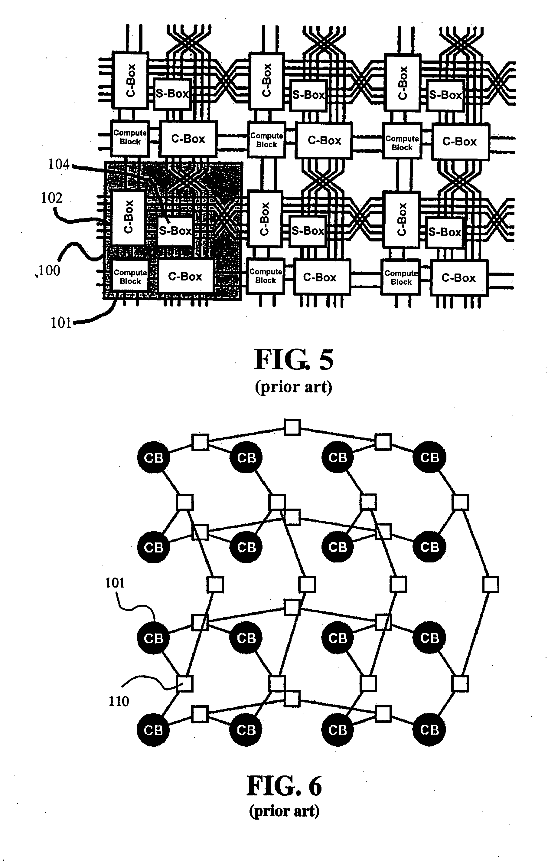
However, such a hierarchical scheme does not eliminate the asymptotic switch requirements.
Conventional experience implementing the Manhattan interconnect scheme has led to the observation that switch requirements tend to be limiting rather than wire requirements.
He did not teach how to parameterize the express cube network or how to lay one out efficiently.

Method used


Image

  • Method and apparatus for network with multilayer metalization
  • Method and apparatus for network with multilayer metalization
  • Method and apparatus for network with multilayer metalization

Examples


Embodiment Construction

The present invention will now be described more fully hereinafter with reference to the accompanying drawings, in which preferred embodiments of the invention are shown. This invention may be embodied in many different forms and should not be construed as limited to the embodiments set forth herein. Further, the dimensions of layers and other elements shown in the accompanying drawings may be exaggerated to more clearly show details. The present invention should not be construed as being limited to the dimensional relations shown in the drawings, nor should the individual elements shown in the drawings be construed to be limited to the dimensions shown.

The asymptotic analysis presented above in regard to the Manhattan interconnection scheme indicates that it is necessary to bound the compute block connections to a constant if the total switches per compute block is to be contained to a constant independent of design size. Certain embodiments according to the present invention ma...


PUM


Abstract

A network for interconnecting processing element nodes which supports rich interconnection while having a number of switching elements which is linear in the number of processing elements interconnected. Processing elements connect to the lowest level of the tree and the higher levels of the tree make connections between the processing elements. The processing elements may be laid out in a two dimensional grid and one or more horizontal and vertical trees may be used to connect between the processing elements with corner switches used to connect between the horizontal and vertical trees. The levels of the tree can be accommodated in multiple layers of metalization such that the entire layout requires a two-dimensional area which is linear in the number of processing elements supported.

Description

BACKGROUND 1. Field The present disclosure describes methods and techniques for interconnecting a collection of processing elements in which multiple metallization layers may be used. For example, the present disclosure describes a method and apparatus for interconnecting compute, memory and / or logic blocks in a Field Programmable Gate Array (FPGA), System-on-a-Chip (SoC), Programmable System-on-a-Chip (PSOC), multi-processor chip, structured Application Specific Integrated Circuits (ASIC), or heterogeneous combinations of such elements. 2. Description of Related Art VLSI technology has advanced considerably since the first gate arrays and FPGAs. Feature sizes have shrunk, die sizes and raw capacities have grown, and the number of metal layers available for interconnect has grown. The most advanced VLSI processes now sport 7-9 metal layers, and metal layers have grown roughly logarithmically in device capacity. Multi-level metalization, and particularly the current rate of scali...

Claims


Application Information

Patent Timeline
IPC IPC(8): G06F15/80H03K19/177
CPCG06F15/8023H03K19/17796H03K19/1778H03K19/17736
Inventor DEHON, ANDRERUBIN, RAPHAEL
Owner CALIFORNIA INST OF TECH
Learn More