
Transimpedance amplifier with adjustable output amplitude and wide input dynamic-range

a transimpedance amplifier and output amplitude technology, applied in the field of analog electronic circuits, can solve the problems of expensive dual voltage sources in order to extend the dynamic range, the limitation of the dynamic range is undesirable for most applications, and the limitation of the amplifier bandwidth requirements

Inactive Publication Date: 2005-03-10
TEXAS INSTR INC
View PDF3 Cites 7 Cited by
  • Summary
  • Abstract
  • Description
  • Claims
  • Application Information

AI Technical Summary

Benefits of technology

The present invention provides an improved transimpedance amplifier that overcomes the limitations of prior art. The circuit includes a feedback resistor with shunt circuitry consisting of two additional transistors, which are driven for example with electrically adjustable voltage sources. The circuit can be portable to virtually any circuit integration process including non-silicon technologies. The output amplitude can be designed with arbitrary dependencies on parameters such as temperature and supply voltage. Additionally, parasitic effects, such as pulse width distortion in overload condition caused by different rise and fall times, can be compensated.

Problems solved by technology

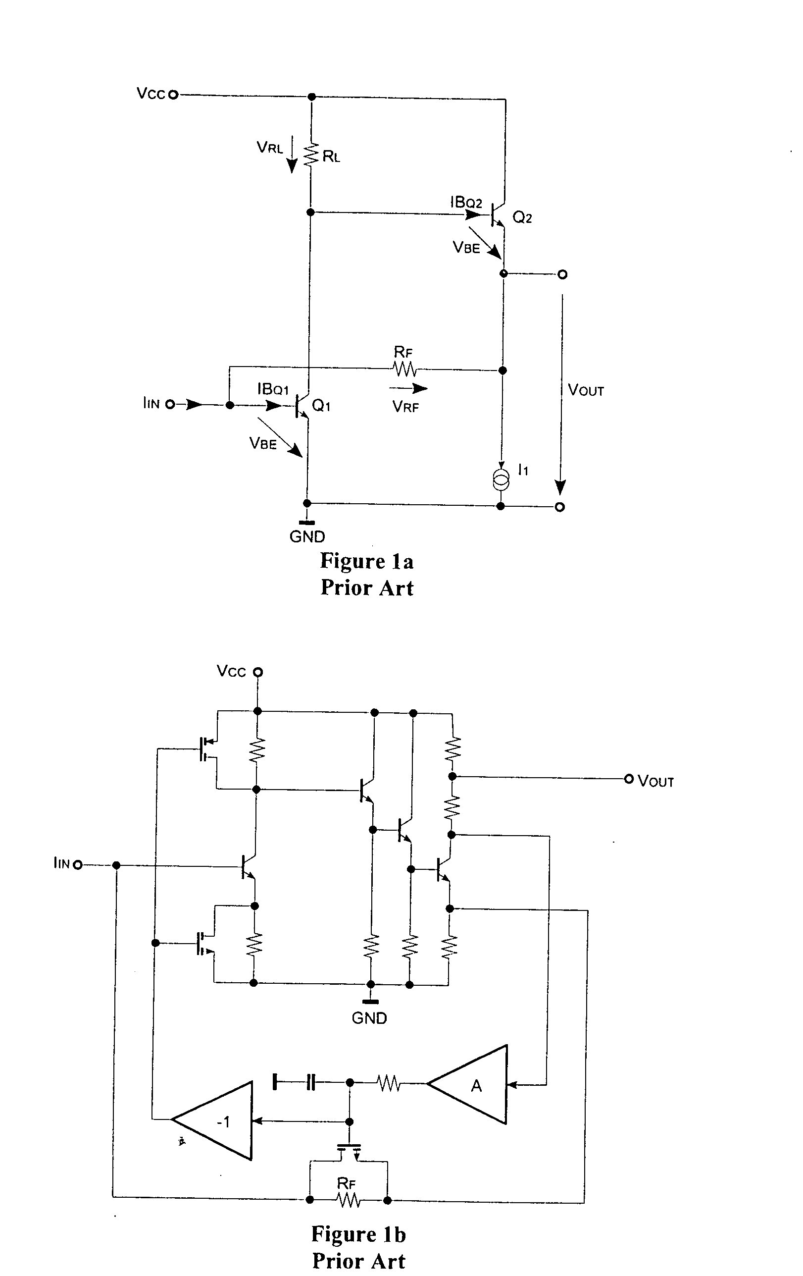
In order to achieve good noise performance, the transimpedance of the amplifier needs to be maximized as far as possible, which is typically limited by the amplifier bandwidth requirements.
Any limitation of the dynamic range is undesirable for most applications.
Also providing dual voltage sources in order to extend the dynamic range is expensive and not practical.
For monolithic integration they require a BiCMOS process with both bipolar and CMOS devices being realized on a single substrate, which is a costly solution.
Additionally, this solution requires a low frequency adaptation loop, which may lead to insufficient performance if the level of the input current varies rapidly, as in burst mode applications.
The same disadvantages hold for the approach disclosed in U.S. Pat. No. 6,583,671 B2: “Stable AGC Transimpedance Amplifier With Expanded Dynamic Range” by J. G. Chatwin. Which also uses MOSFET devices in parallel to the transimpedance feedback resistor.
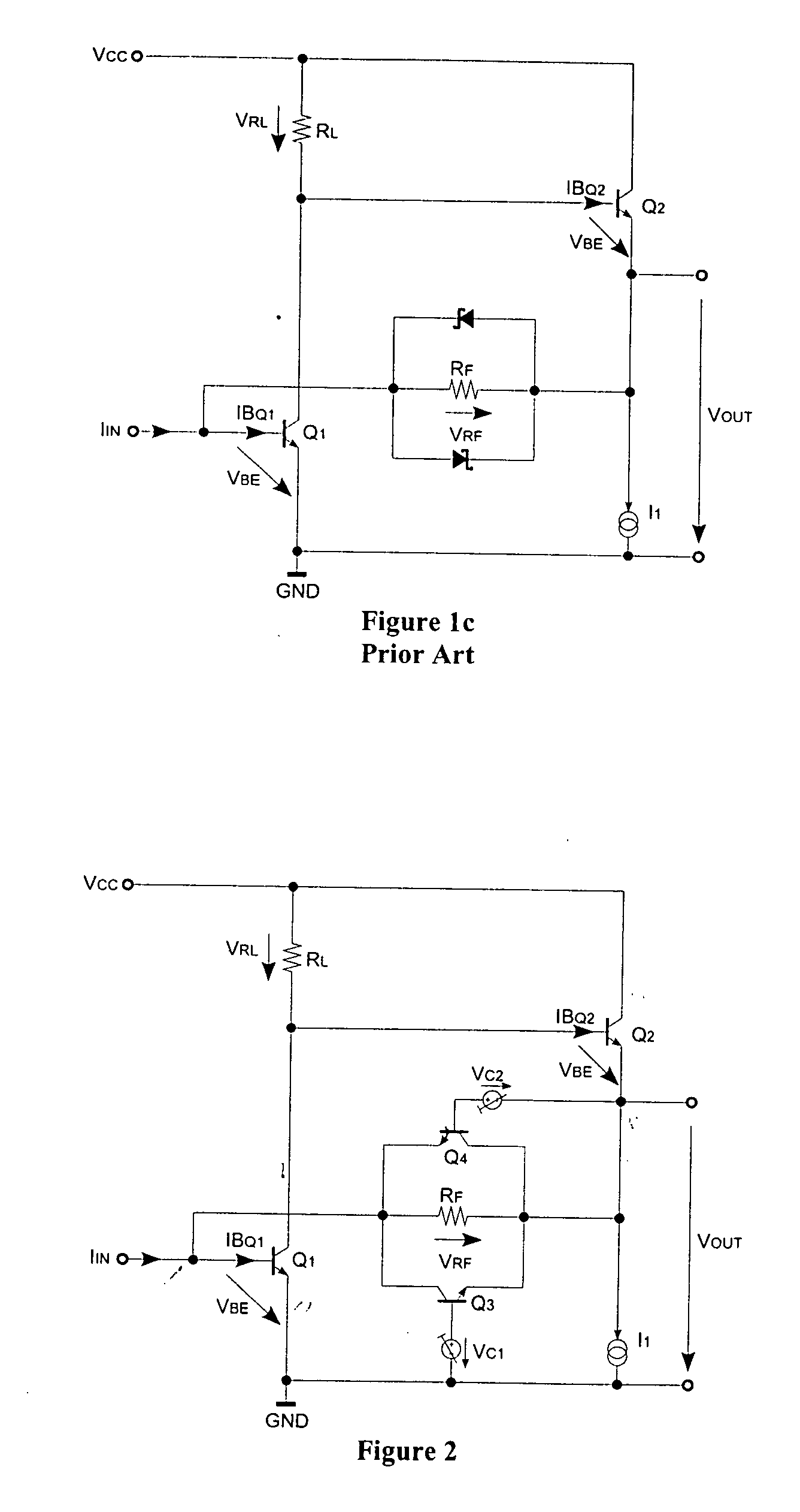
However, this solution suffers from several disadvantages: While diodes are always available in bipolar technologies, the preferred Schottky diodes do not exist in modern bipolar technologies, because in today's technologies for connection of the devices polysilicon is used below the metallization.
The voltage drops across diodes, however, equals the base-emitter voltage drop of bipolar transistors, leading to operating point problems in the circuit given in FIG. 1c.
Furthermore, the diode voltage drop is highly temperature dependent.

Method used


Image

  • Transimpedance amplifier with adjustable output amplitude and wide input dynamic-range
  • Transimpedance amplifier with adjustable output amplitude and wide input dynamic-range
  • Transimpedance amplifier with adjustable output amplitude and wide input dynamic-range

Examples


Embodiment Construction

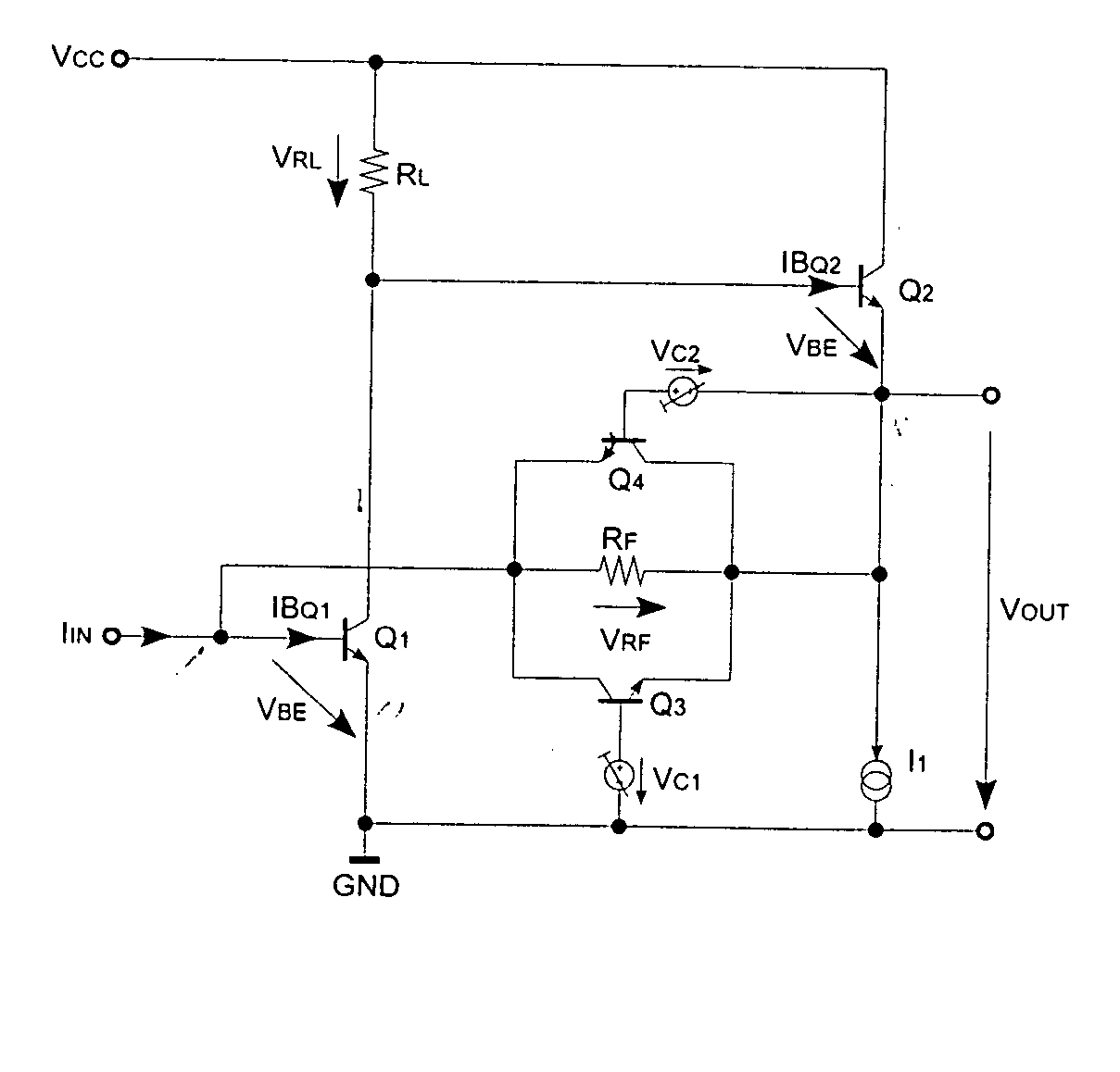
[0024] An integratable transimpedance amplifier with adjustable limited output voltage and wide input-current dynamic range according to an embodiment of the present invention is shown in FIG. 2. The circuit arrangement includes a transimpedance amplifier consisting of transistors, a constant current source a load resistor and the feedback resistor with a shunt circuitry consisting of the additional transistors, which are driven for example with electrically adjustable voltage sources.

[0025] The embodiment shown in FIG. 2 provides a bipolar all npn implementation of the present invention. The amplifier stage consists of a common emitter input transistor Q1, with the input current signal IIN connected to the base node, and the collector of said transistor connected to the positive supply voltage VCC by means of a load resistor RL. A second transistor Q2 with its base connected to the collector of the first transistor operates as an emitter follower. The collector of the second trans...


PUM


Abstract

A transimpedance amplifier circuit comprising transistors, a constant current source, a load resistor, and the feedback resistor with a shunt circuitry consisting of the additional transistors, which are driven for example with electrically adjustable voltage sources. In a bipolar npn implementation the amplifier stage consists of a common emitter input transistor Q1, a transistor Q2 with its base connected to the collector of the first transistor operates as an emitter follower. A resistor RF connected between the emitter of said second transistor and the base of said first transistor provides a voltage controlled current feedback from the amplifier output to its input. The output voltage VOUT is generated at the emitter node of said second transistor. A shunt circuitry consists of a third and a fourth transistor Q3 and Q4 connected in shunt across resistor RF. In an embodiment, the base node voltages of the transistors Q3 and Q4 are adjusted by control voltage sources. By means of an appropriate implementation of these voltage sources the maximum and minimum limits of the output voltage VOUT is defined, which can easily be implemented with arbitrary temperature or supply voltage dependency.

Description

TECHNICAL FIELD OF THE INVENTION [0001] In general this invention applies to analog electronic circuits. More particularly it relates to transimpedance amplifiers. BACKGROUND OF THE INVENTION [0002] Transimpedance amplifiers are used to amplify and convert current signals to voltage signals. The input current source typically shows high impedance at low frequencies, which in most applications is shunted by parasitic capacitances. These capacitances lower the source impedance at higher frequencies. As a result it is advantageous for a transimpedance amplifier to provide low input impedance over a wide frequency range. [0003] In broadband fiber-optical data transmission systems, transimpedance amplifiers are, for example, driven by photodiodes. In dependence of the light intensity at the fiber input and dependent on the length and the quality of the fiber interconnect the current generated by the photodiode can vary by several orders of magnitude. [0004] In order to achieve good noise...

Claims


Application Information

Patent Timeline
Patent Type & Authority Applications(United States)
IPC IPC(8): H03F1/34H03F3/08
CPCH03F3/08H03F1/34
Inventor SCHMIDT, LOTHARMUTH, KARLHEINZBRAIER, MARTIN
Owner TEXAS INSTR INC
Learn More