Clock distribution networks and conductive lines in semiconductor integrated circuits

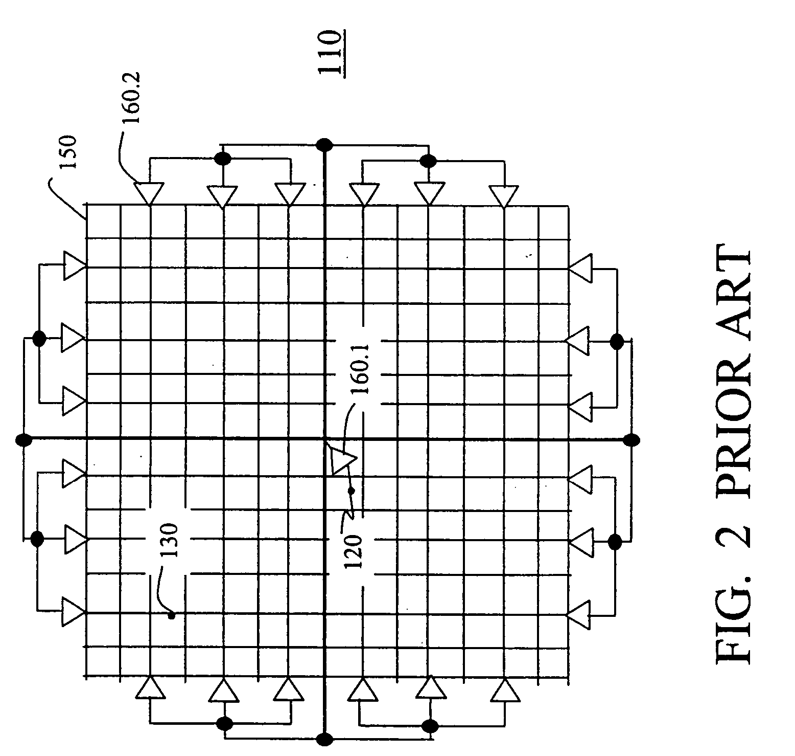
a technology of clock distribution network and semiconductor integrated circuit, which is applied in the direction of generating/distributing signals, instruments, basic electric elements, etc., can solve the problems of difficult control of the impedance of lines b>150, the perfect placement of the clock distribution network on the semiconductor die, and the clock propagation speed. the effect of lowering the rc value of lines 150

Inactive Publication Date: 2005-03-10
INVENSAS CORP
View PDF36 Cites 4 Cited by
  • Summary
  • Abstract
  • Description
  • Claims
  • Application Information

AI Technical Summary

Benefits of technology

[0015] In some embodiments, the clock distribution lines 150 (FIGS. 1, 2) are formed in trenches etched in a semiconductor substrate. The RC value of lines 150 can be lowered by making the trenches deeper, without increasing the lateral area occupied by the RC lines. Also, the RC value, and hence the clock skew, become more controllable.

Problems solved by technology

A perfect placement of a clock distribution network on a semiconductor die can be difficult due to the presence of other circuitry.
As a result, it is difficult to control the impedance of lines 150 and therefore the clock propagation speed.
Further, the ground plane or grid consumes valuable area, increases the cost and complexity of the integrated circuit, and sometimes does not completely eliminate the electromagnetic interference problem because the position of the ground plane or grid can be restricted to allow the same metal layer to be used for other circuit elements.
The small angles when combined with small spacing between a line 324 or 326 and a line 150 may lead to significant electromagnetic interference and parasitic capacitance.

Method used


Image

  • Clock distribution networks and conductive lines in semiconductor integrated circuits
  • Clock distribution networks and conductive lines in semiconductor integrated circuits
  • Clock distribution networks and conductive lines in semiconductor integrated circuits

Examples


Embodiment Construction

[0030] The examples in this section are provided for illustration and not to limit the invention. The invention is not limited to particular circuits, materials, processes, process parameters, equipment, or dimensions.

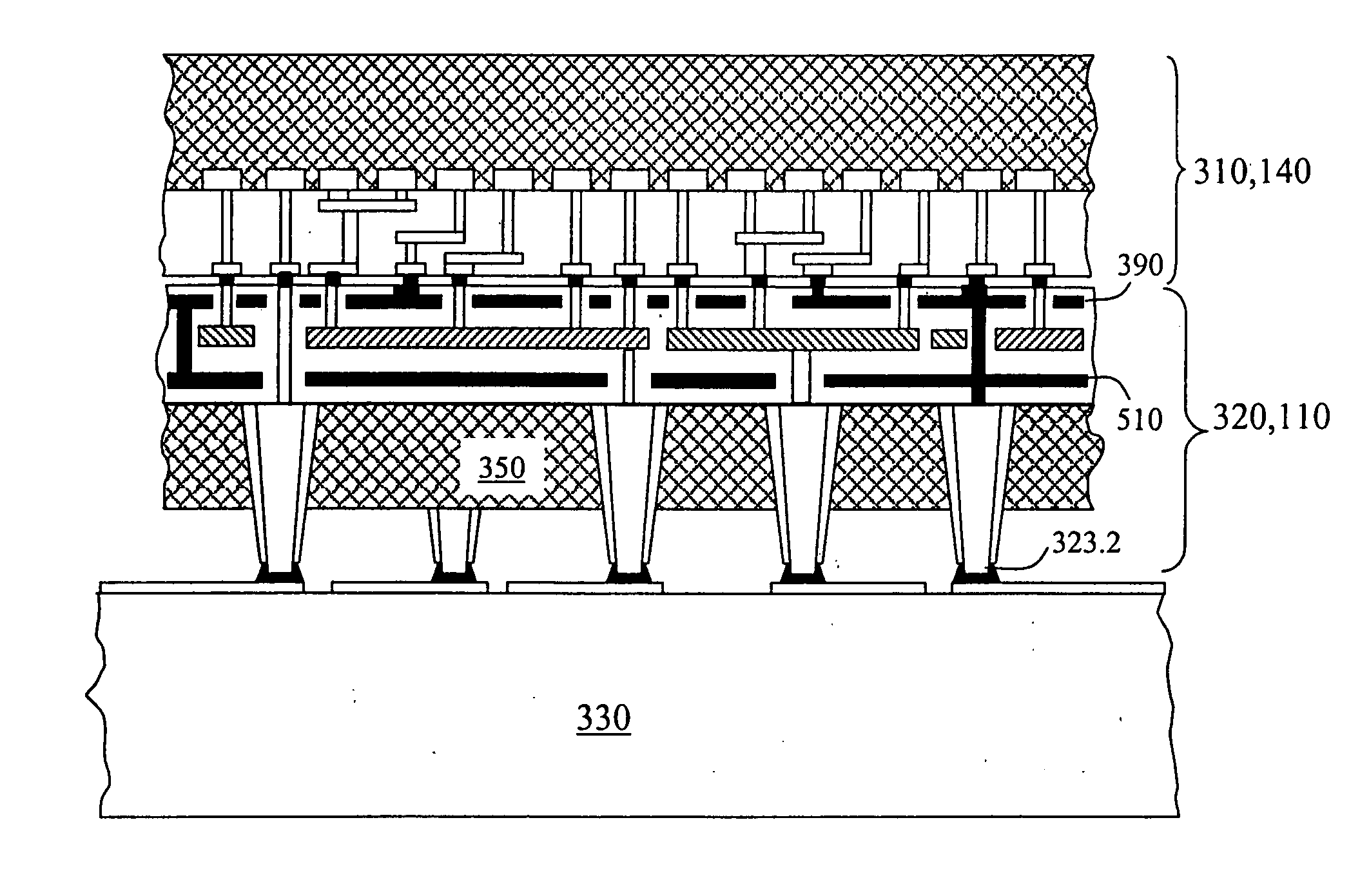
[0031]FIG. 4 illustrates an integrated circuit 310 mounted on another integrated circuit 320 which in turn is mounted on a wiring substrate 330. Each of circuits 310, 320 is a semiconductor die or wafer, or some portion of a semiconductor wafer. Circuit 310 includes clocked circuitry 140 and may also include non-clocked circuitry. For example, circuit 310 may include a microprocessor, a memory, a digital controller, and so on. Circuit 320 is an interposer that contains clock distribution networks 110. The clock distribution networks can be of any type, including the types shown in FIGS. 1, 2, or other types, known or to be invented.

[0032] Circuit 310 includes a semiconductor substrate 340. Active areas 340A may have been formed in substrate 340 for transistors, resis...


PUM


Abstract

A clock distribution network (110) is formed on a semiconductor interposer (320) which is a semiconductor integrated circuit. An input terminal (120) of the clock distribution network is formed on one side of the interposer, and output terminals (130) of the clock distribution network are formed on the opposite side of the interposer. The interposer has a through hole (360), and the clock distribution network includes a conductive feature going through the through hole. The side of the interposer which has the output terminals (130) is bonded to a second integrated circuit (310) containing circuitry clocked by the clock distribution network. The other side of the interposer is bonded to a third integrated circuit or a wiring substrate (330). The interposer contains a ground structure, or ground structures (390, 510), that shield circuitry from the clock distribution network. Conductive lines (150) in an integrated circuit are formed in trenches (610) in a semiconductor substrate.

Description

BACKGROUND OF THE INVENTION [0001] The present invention relates to placement of clock distribution networks and fabrication of conductive lines in semiconductor integrated circuit structures. [0002]FIG. 1 shows a tree-like clock distribution network 110 designed to distribute a clock signal with a minimum clock skew in an integrated circuit. The clock signal is received at a terminal 120 and distributed to terminals 130 at the leaves of tree 110. Terminals 130 are connected to inputs of circuit blocks 140 such as registers, flip flops, latches, logic gates, etc. The network tree is provided by conductive lines 150. The wires 150 that connect the tree nodes of each given tree level to the tree nodes of any given adjacent level have the same dimensions. Buffers (amplifiers) 160 are located at selected points in the tree to amplify the clock signal. In order to minimize the clock skew, each clock path from terminal 120 to a terminal 130 has the same dimensions, and the respective buff...

Claims


Application Information

Patent Timeline
Patent Type & Authority Applications(United States)
IPC IPC(8): G06F1/10G11C7/00H01L21/44H01L21/4763H01L21/48H01L21/50H01L21/56H01L23/31H01L23/498H01L23/52H01L23/528H01L27/10H01L29/739H01L31/00
CPCG06F1/10H01L2924/01019H01L21/563H01L21/568H01L23/3121H01L23/3128H01L23/481H01L23/49833H01L23/528H01L23/5283H01L2224/73203H01L2924/19041H01L2924/3011H01L2924/3025H01L24/97H01L2224/16225H01L21/561H01L24/05H01L2224/05001H01L2224/05008H01L2224/05009H01L2224/05023H01L2224/05024H01L2224/0557H01L2224/05571H01L2224/05573H01L2924/12042H01L2924/14H01L2924/00
Inventor SINIAGUINE, OLEG
Owner INVENSAS CORP
Why Eureka
Try Eureka