Method and system for nanoscale plasma processing of objects

a plasma processing and nano-scale technology, applied in the field of plasma processing of objects, can solve the problems of short plasma/substrat interaction time, inacceptable plasma processing of layers with nano-scale dimensions, and several current technologies, etc., and achieve the effect of allowing control of interaction tim

Inactive Publication Date: 2005-03-10
MARYLAND UNIV OF
View PDF4 Cites 71 Cited by
  • Summary
  • Abstract
  • Description
  • Claims
  • Application Information

AI Technical Summary

Benefits of technology

It is therefore an object of the present invention to provide nanoscale plasma processing of a workpiece which permits control of interaction time between a workpiece and a fully established stable plasma.
At the end of the desired plasma interaction time, the substrate is shielded from further exposure to the plasma by moving the shutter (or the substrate) back into its original position. Alternatively, with a slit formed in the shutter, a controlled linear motion of the shutter and / or substrate will be sufficient to prevent exposure of the substrate to the plasma at undesired periods. This approach enables precise, short time, nanoscale plasma processing. The shutter is positioned in close proximity to the substrate (about 0-1 mm therebetween) in order to minimize, or completely eliminate, the volume located between the shutter and the substrate. In this fashion, the change in volume that the plasma experience when the shutter is removed is minimized, and the plasma properties remain nearly constant. The present invention enables the interaction of the substrate with a fully established, well-defined, stable plasma for tightly controlled exposure times (from fractions of a second to many seconds) required for nanoscale processing of materials.

Problems solved by technology

Because of the nanoscale thickness of the material layers that need to be added, modified or removed, the plasma / substrate interaction time has to be short.
Current technology suffers from several disadvantages when applied to plasma processing of nanoscale layers.
This is acceptable for the processing of thick layers, but not acceptable for plasma processing of layers with nanoscale dimensions.
Any changes of the substrate introduced by the inadvertent interaction of the substrate with the plasma during one of the undesirable periods, such as initialization of the plasma, biasing of the substrate, stabilizing plasma, plasma extinction, and decay of long leaved neutrals, may reduce the efficacy of the plasma process.
This deposition process can have unacceptable consequences for profile control of ultra-fine features.
Another drawback of the current plasma processing, is that the etching depth and / or film thickness of deposited films is not well controlled because of the sequential and additive effects of different regimes of the plasma / surface interaction.
Obviously, this approach increases process complexity, and for plasma processing of substrates with nanoscale dimensions may be impractical, if not impossible.
The disadvantage of the thin film processing equipment described in the U.S. Pat. No. 6,132,805, is that the shutter is located an extended distance from the substrate, and the system uses the plasma generation between the shutter and the substrate.
This is undesirable for nanoscale plasma processing where the exposure time of the substrate to any kind of plasma or reactive environment must be precisely controlled.
This control of the short time interaction of a substrate with a fully established and stable plasma is not possible in the system described in the U.S. Pat. No. 6,132,805 since the existence of a large volume between the shutter and the substrate causes appreciable changes in the plasma once the shutter is removed from the substrate for processing.
Another deficiency of the prior plasma processing techniques is that if a microscopic shutter is used to control the exposure time of the substrate to a plasma, either by movement of the shutter or of the substrate relative to the shutter, a sheath will form at the surfaces of the shutter.
The problem is that orientation of the sheath may be directed parallel to a normal of the substrate which prevents the ion bombardment of the substrate.
The use of the microscopic shutters in the plasma processing becomes problematic if a very short time exposure of a substrate to the plasma is required, i.e., for nanoscale layer processing or for diagnostics of the plasma.

Method used


Image

  • Method and system for nanoscale plasma processing of objects
  • Method and system for nanoscale plasma processing of objects
  • Method and system for nanoscale plasma processing of objects

Examples


Embodiment Construction

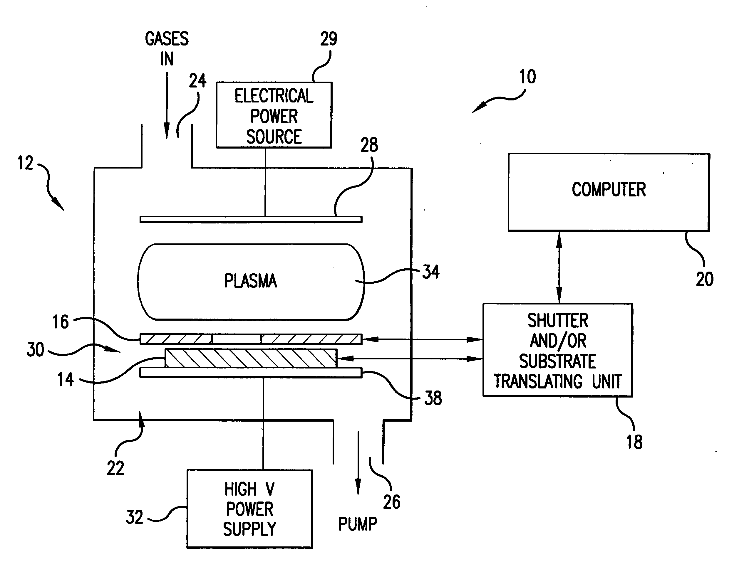
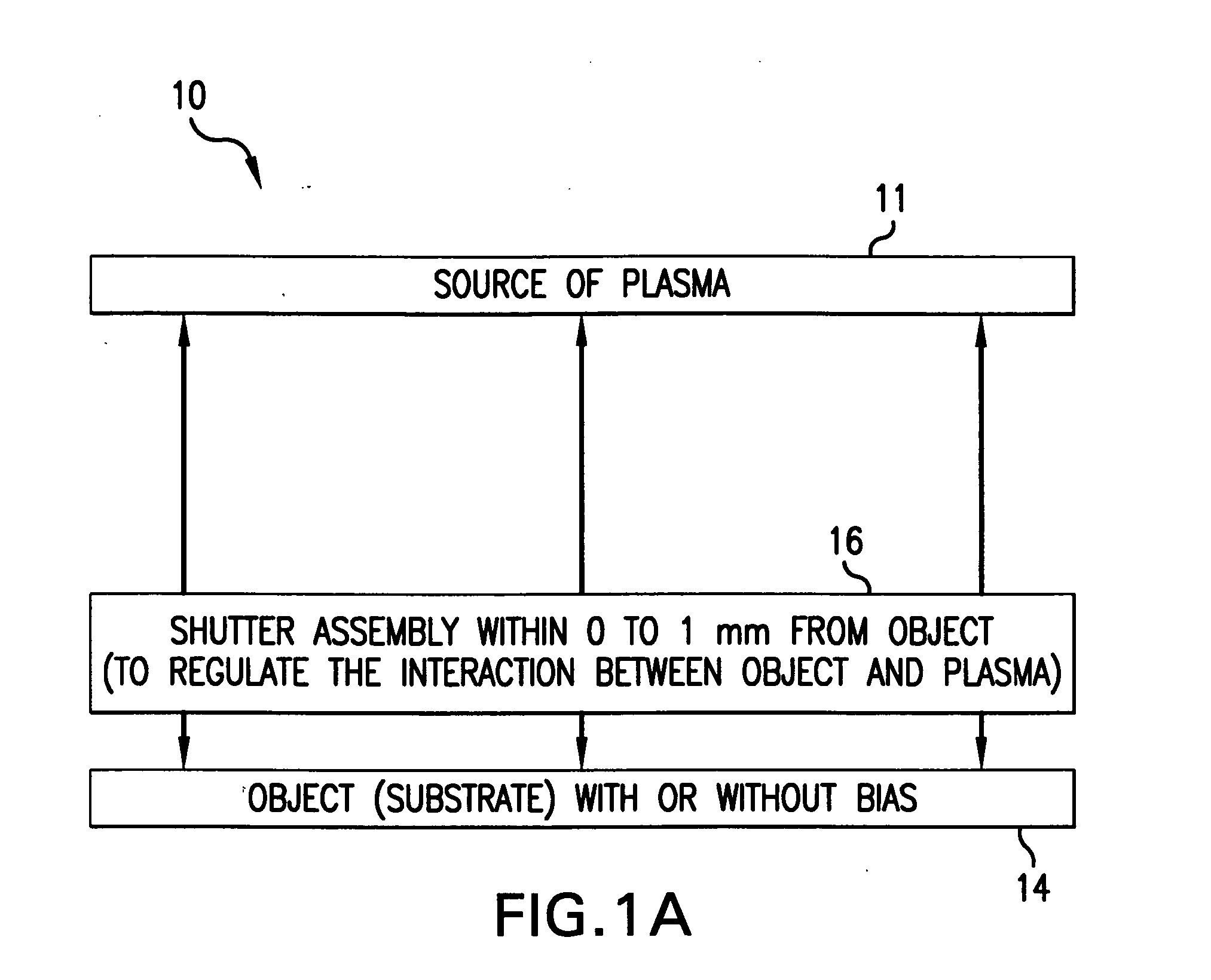
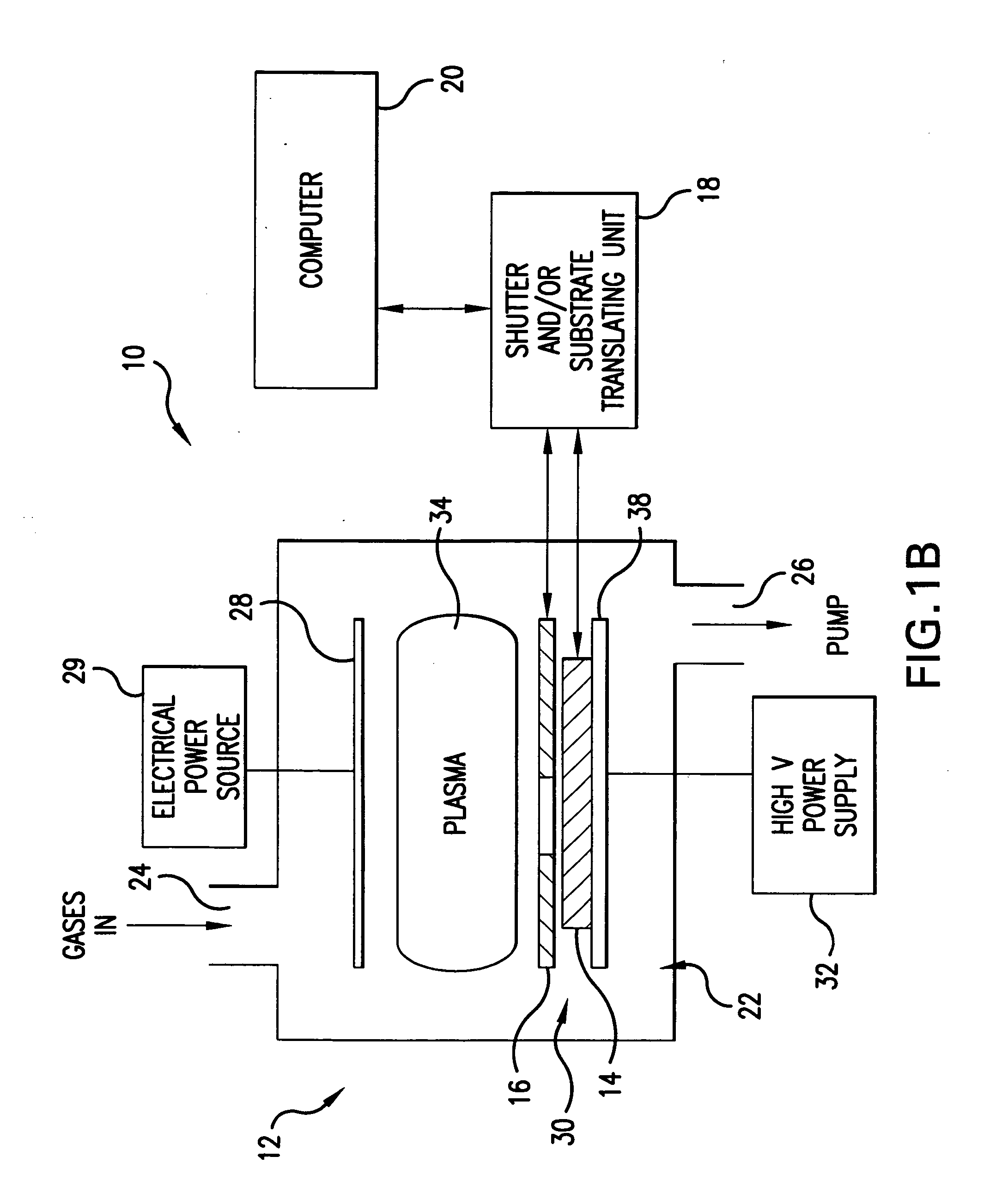
Referring to FIGS. 1A and 1B, there is shown a system 10 for nanoscale plasma processing of a workpiece including a source of plasma 11 (also referred to herein as plasma generating unit), a plasma reactor 12, the details of which will be presented infra herein; a workpiece 14, also referred herein as a substrate or an object; a shutter assembly 16 in close proximity or in contiguous relationship with the substrate 14; a shutter and / or substrate translating unit 18; and a computer 20 controlling the operation of the system 10. The plasma reactor 12 includes a plasma processing chamber 22 filled with gas molecules (for example, Ar) passing through a gas inlet 24. As an example, the reactive gas pressure within the plasma processing chamber 22 may be maintained at between approximately 1 mTorr and 10 Torr. Also, atmospheric pressure discharges are contemplated in the system of the present invention for many low-tech materials. The pressure parameters discussed supra are an example of...


PUM

PropertyMeasurementUnit
Widthaaaaaaaaaa
Widthaaaaaaaaaa
Widthaaaaaaaaaa

Abstract

A plasma processing system includes a source of plasma, a substrate and a shutter positioned in close proximity to the substrate. The substrate / shutter relative disposition is changed for precise control of substrate / plasma interaction. This way, the substrate interacts only with a fully established, stable plasma for short times required for nanoscale processing of materials. The shutter includes an opening of a predetermined width, and preferably is patterned to form an array of slits with dimensions that are smaller than the Debye screening length. This enables control of the substrate / plasma interaction time while avoiding the ion bombardment of the substrate in an undesirable fashion. The relative disposition between the shutter and the substrate can be made either by moving the shutter or by moving the substrate.

Description

FIELD OF THE INVENTION The present invention relates to plasma processing of objects, and specifically to nanoscale processing of thin films and substrates by exposing the substrates to electrically charged plasmas for surface modifications. In overall concept thereof, the present invention relates to processing of objects of micro-electronics, specifically for etching, deposition, etc. of thin films and substrates by plasma processing, and particularly to the control of the interaction time between the plasma and work pieces to assure optimum quality of the resulting structures. In more detail, the present invention relates to a plasma processing system in which a shutter is positioned in a plasma processing chamber in close proximity to a work piece. The relative disposition between the shutter and the work piece is controlled to either shield the work piece from the plasma or to allow exposure of the work piece to the plasma for the desired interaction time when the plasma is ...

Claims


Application Information

Patent Timeline
IPC IPC(8): H01J37/32
CPCH01J37/32623
Inventor OEHRLEIN, GOTTLIEB S.HUA, XUEFENGSTOLZ, CHRISTIAN
Owner MARYLAND UNIV OF
Why Eureka
Try Eureka