
Display device

a technology for display devices and light emitting devices, which is applied in the field of display devices, can solve the problems of increasing varying the power consumption of light emitting devices in turn, so as to suppress the effect of preventing the increase of the power consumption of light emitting devices

Inactive Publication Date: 2005-01-27
SEMICON ENERGY LAB CO LTD
View PDF64 Cites 79 Cited by
  • Summary
  • Abstract
  • Description
  • Claims
  • Application Information

AI Technical Summary

Benefits of technology

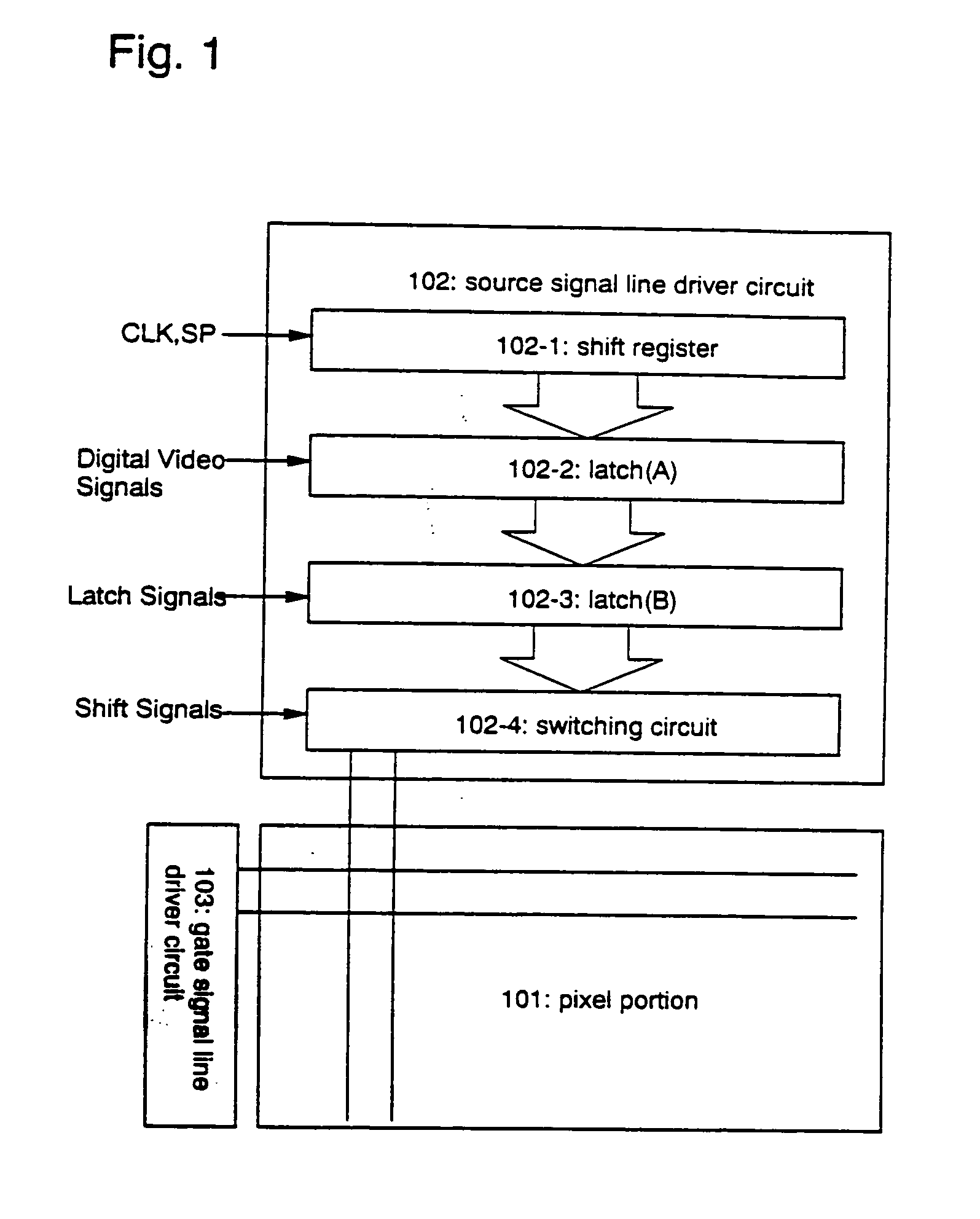
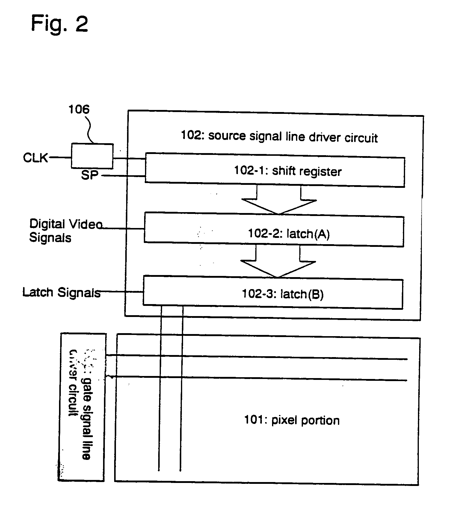
The present invention provides a display device that can reduce power consumption by controlling the contrast of an image based on the type of image being displayed. This is done by using a pixel portion that includes a plurality of pixels, and a source signal line driver circuit that inputs a digital video signal to the pixels. The number of bits of the digital video signal that is input into the pixels is reduced, which in turn reduces the power consumption of the light emitting device. Additionally, the invention provides a display device that can perform a digitally-driven time-divisional gradation display with reduced power consumption by reducing the number of bits of the digital video signal that is input into the pixels. The invention also includes a light emitting element that monitors the temperature and maintains a constant current level, resulting in a constant brightness of the pixels even when the environmental temperature changes. Overall, the invention provides a display device that can reduce power consumption and maintain brightness levels, improving the efficiency of the display device.

Problems solved by technology

Consequently, power consumption of a group of driver circuits to be used for inputting the digital video signal into the pixels is increased, thereby resulting in increased power consumption of the light emitting device.
Accordingly, power consumption of the light emitting device in turn varies depending on an image to be displayed.
Accordingly, as an environmental temperature under which the light emitting element is to be used increases, power consumption of the light emitting device increases, which in turn increases the brightness of the light emitting element.

Method used


Image

  • Display device
  • Display device
  • Display device

Examples


embodiment

[0117] [Embodiment Mode 4]

[0118] Still another example of the second structure in accordance with the present invention, which is different from the ones described in Embodiment Modes 2 and 3, will be now described. FIG. 4 shows a block diagram of a light emitting device having the second structure in accordance with the present invention. In FIG. 4, the same components as shown in FIG. 1 are designated with the same reference numerals.

[0119] The light emitting device in the present embodiment mode employs a start pulse signal control circuit 108 which allows a constant electrical potential, instead of the start pulse signal (SP), to be applied to the shift register 102-1.

[0120] More specifically, the light emitting device is configured to input a constant electrical potential (fixed electrical potential) into the shift register 102-1, instead of the start pulse signal, for a constant time period by means of the start pulse signal control circuit 108, so that the timing signal tha...

embodiment 1

[0136] [Embodiment 1]

[0137] In the present embodiment, the structure of a pixel portion of a light emitting device and its driving method in accordance with the present invention will be described.

[0138]FIG. 6 shows an expanded view of the pixel portion 301 of the light emitting device in accordance with the present embodiment of the invention. Source signal lines (S1 to Sx), power source lines (V1 to Vx), and gate signal lines (G1 to Gy) are provided in the pixel portion 301.

[0139] In the present embodiment, a pixel 304 refers to a region in which one of the source signal lines (S1 to Sx), one of the power source lines (V1 to Vx), and one of the gate signal lines (G1 to Gy) are provided. In the pixel portion 301, a plurality of the pixels 304 are arranged in matrix.

[0140] An expanded view of the pixel 304 is shown in FIG. 7. In FIG. 7, reference numeral 305 denotes a switching TFT. A gate electrode of the switching TFT 305 is connected to the gate signal line G (G1 to Gx). One o...

embodiment 2

[0164] [Embodiment 2]

[0165] In the present embodiment, another example of the structure of a pixel portion of a light emitting device and its driving method in accordance with the present invention, different from those in the Embodiment 1, will be described.

[0166]FIG. 9 shows an exemplary block diagram of a light emitting device in the present embodiment. The light emitting device in FIG. 9 includes a pixel portion 901 by TFT formed on the substrate and includes a source signal side driver circuit 902, a writing gate signal side driver circuit (first gate signal line driver circuit) 903a, and an erasure gate signal line driver circuit (second gate signal line driver circuit) 903b, each provided in the periphery of the pixel portion. Although the light emitting device with one source signal side driver circuit is described in the present embodiment, two of the source signal side driver circuits may be provided.

[0167] The source signal side driver circuit 902 has at least one of th...


PUM


Abstract

The present invention is intended to suppress power consumption of an EL display. In accordance with the brightness of an image to be displayed in a pixel portion, the contrast of the image is determined whether to be inverted or not, and the number of bits of the digital video signal to be input into the pixel portion is reduced, and the magnitude of a current to flow through the EL element is allowed to be maintained at a constant level even when a temperature of an EL layer changes by providing the EL display with another EL element to be used for monitoring a temperature.

Description

BACKGROUND OF THE INVENTION [0001] 1. Field of the Invention [0002] The present invention relates to a display panel in which a light emitting element formed on a substrate is sealed between the substrate and a cover member. In addition, the present invention also relates to a display module in which an IC chip is mounted on the above-mentioned display panel. It should be noted that in the present specification, the display panel and the display module are collectively referred to as the light emitting device. The present invention further relates to an electronic apparatus that employs the above-mentioned light emitting device. [0003] 2. Description of the Related Art [0004] Recently, techniques for forming a TFT on a substrate has been greatly advanced, and much developments have been made to apply those techniques to an active-matrix type display device. In particular, a TFT employing a poly-crystalline silicon film can operate at a higher speed since a field effect mobility (sim...

Claims


Application Information

Patent Timeline
Patent Type & Authority Applications(United States)
IPC IPC(8): G03B19/02G09G3/30G09F3/00G09F9/30G09G3/10G09G3/20G09G3/32G09G5/00H04B1/00H04M1/00H04N5/225H05B33/00H05B33/14
CPCG09G3/2022H01L27/3244G09G3/3266G09G3/3291G09G2300/0842G09G2300/0866G09G2310/0251G09G2310/0262G09G2310/027G09G2310/0281G09G2320/029G09G2320/041G09G2320/043G09G2330/021G09G2330/028H01L27/32G09G3/3258H10K59/12G09G3/30G09G3/20H10K59/00
Inventor YAMAZAKI, SHUNPEIKOYAMA, JUNOSAME, MITSUAKIOSADA, MAI
Owner SEMICON ENERGY LAB CO LTD
Learn More