
Performance PCRAM cell

a ram and memory technology, applied in the direction of bulk negative resistance effect devices, semiconductor devices, electrical equipment, etc., can solve the problems of shrinking the size of each element, volatile ram devices, and loss of stored data

Inactive Publication Date: 2005-01-27
MICRON TECH INC
View PDF99 Cites 33 Cited by
  • Summary
  • Abstract
  • Description
  • Claims
  • Application Information

AI Technical Summary

Benefits of technology

The invention provides a resistance variable memory element and a method of forming it. The memory element includes a metal-containing layer and a silver layer formed between a first chalcogenide glass layer and a second glass layer. The layers can be doped with a metal and a stack of layers can contain one or more metal-containing layers in serial contact with each other and a silver layer. The invention also provides a plurality of alternating layers of chalcogenide glass layers, metal-containing layers, and silver layers, where the layers start with a first chalcogenide glass layer and end with a last chalcogenide glass layer, with the metal-containing layers comprising a silver-chalcogenide, such as silver-selenide. The invention can provide a memory element with improved resistance to programming and erasing.

Problems solved by technology

Typically, RAM devices are volatile, in that stored data is lost once the power source is disconnected or removed.
Accordingly, the size of each element has been shrinking, which in the case of DRAMs also shortens the element's data holding time.
However, with increasing element number and density, it is becoming more and more difficult to refresh all memory elements at least once within a refresh period.
In addition, refresh operations consume power.
Heat processing can result in substantial amounts of silver migrating into the memory element uncontrollably.
Excessive silver incorporated into the memory element may result in faster degradation, i.e., a short life, and eventually, device failure.

Method used


Image

  • Performance PCRAM cell
  • Performance PCRAM cell
  • Performance PCRAM cell

Examples


first embodiment

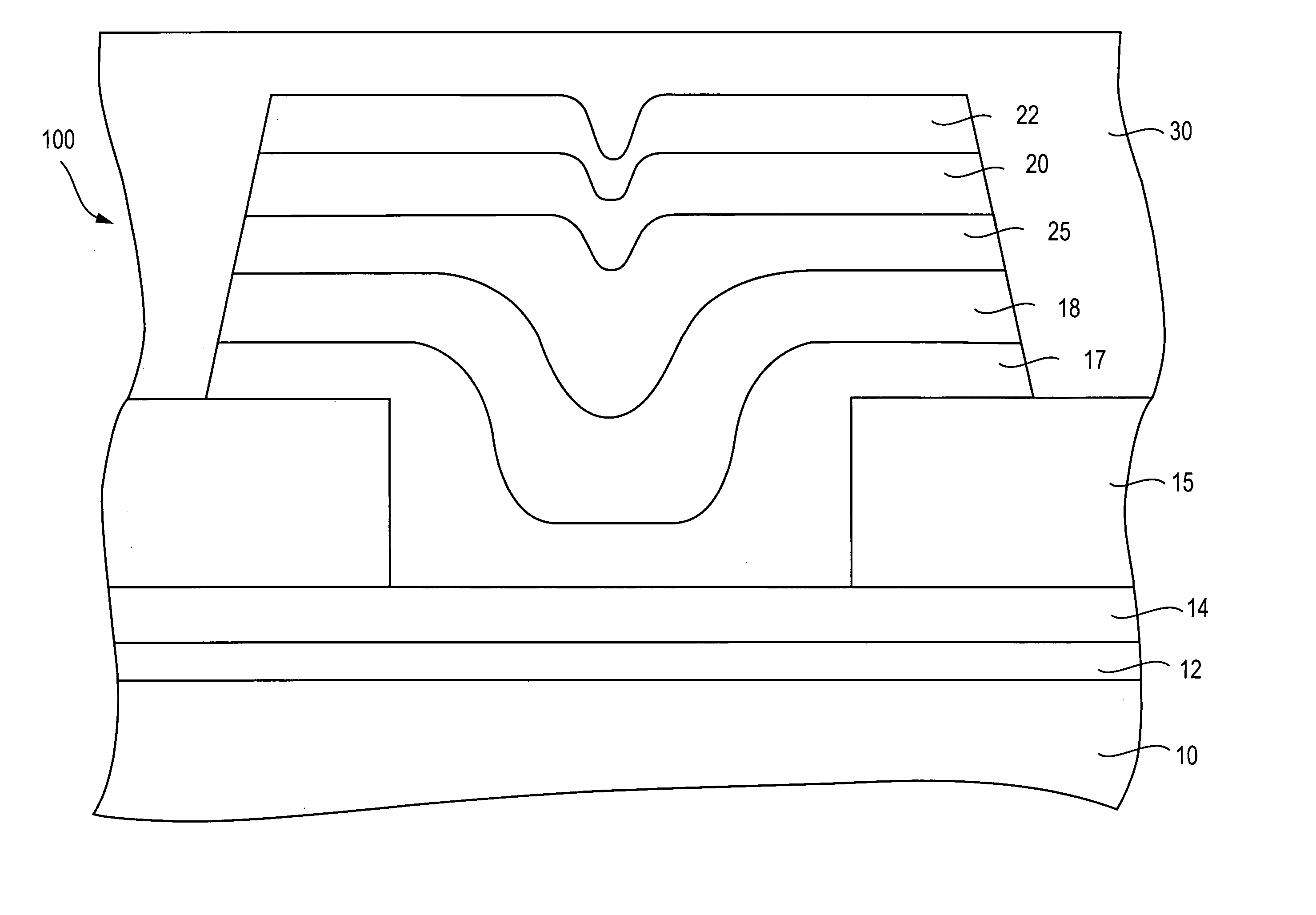
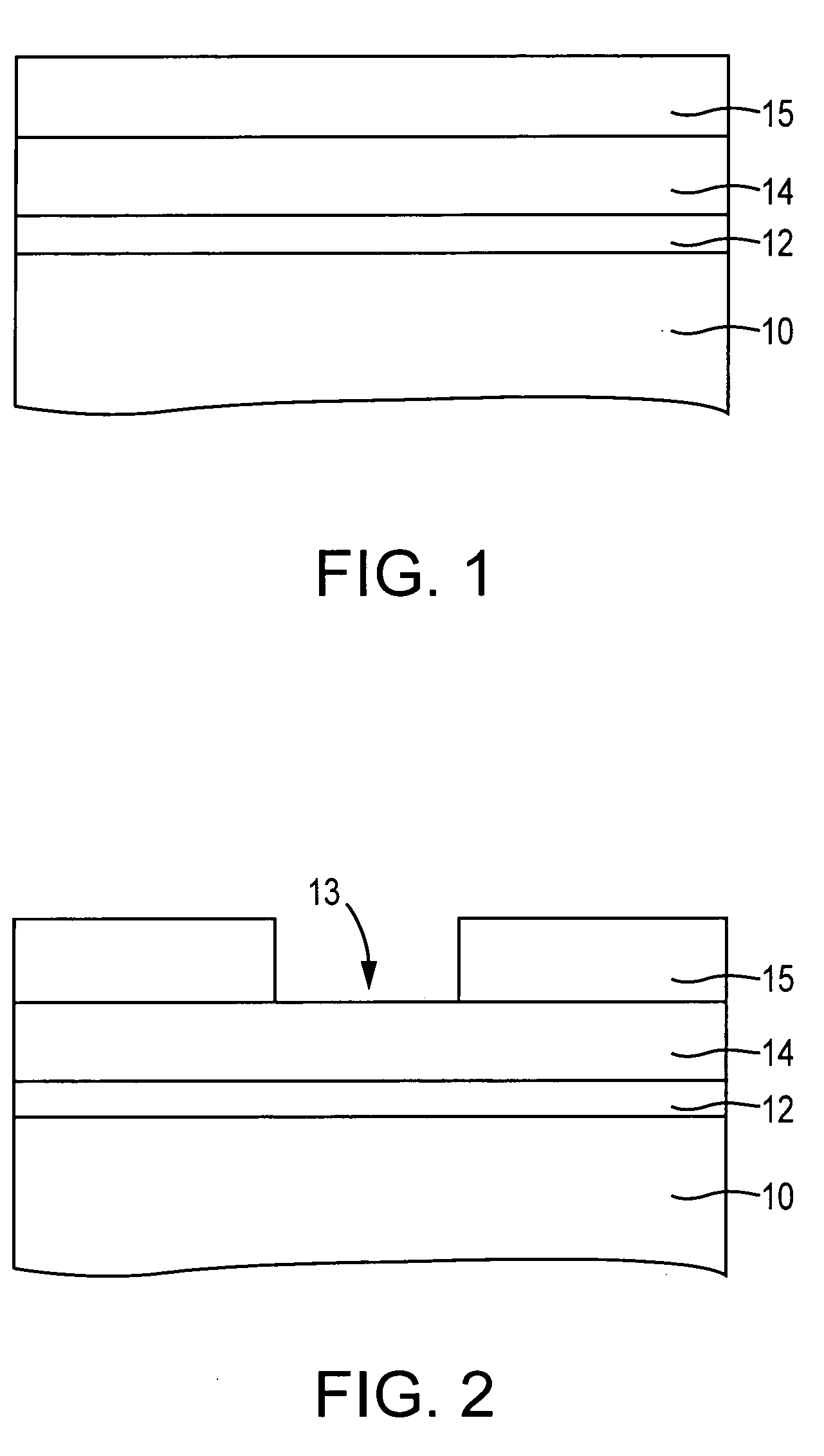
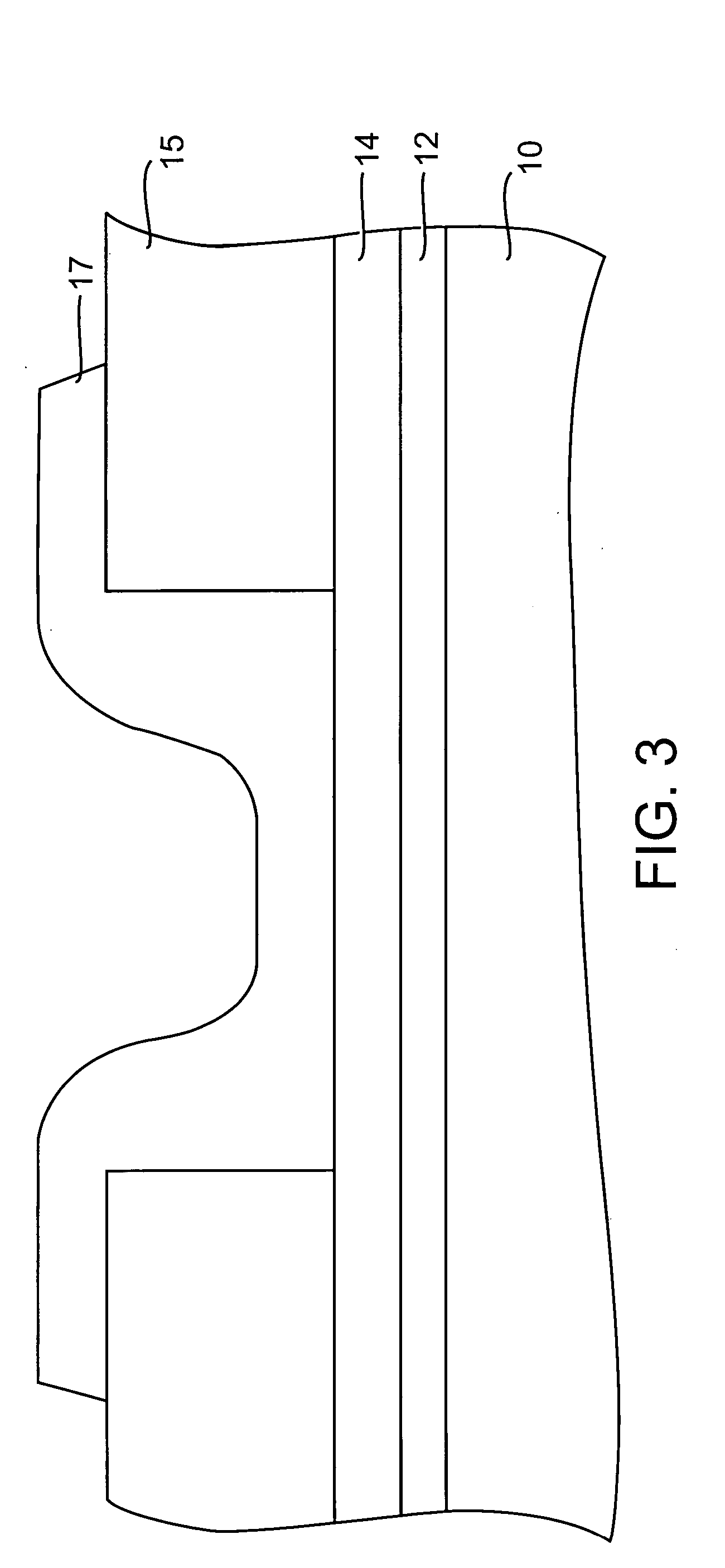
[0039] According to the invention, the first chalcogenide glass layer 17 is a germanium-selenide glass having a GexSe100-x stoichiometry. The preferred stoichiometric range is between about Ge20Se80 to about Ge43Se57 and is more preferably about Ge40Se60. The first chalcogenide glass layer 17 preferably has a thickness of from about 100 Å to about 1000 Å, and more preferably has a thickness of about 150 Å.

[0040] The first chalcogenide glass layer serves as a glass backbone for allowing a metal-containing layer, such as a silver-selenide layer, to be directly deposited thereon. The use of a metal-containing layer, such as a silver-selenide layer, in contact with the chalcogenide glass layer makes it unnecessary to provide a metal (silver) doped chalcogenide glass, which would require photodoping of the substrate with ultraviolet radiation. However, it is possible to also metal (silver) dope the chalcogenide glass layer, which is in contact with the silver-selenide layer, as an option...

second embodiment

[0056] Referring now to FIG. 9, which shows the invention subsequent to the processing step shown in FIG. 4, the stack of layers formed between the first and second electrodes may include alternating layers of chalcogenide glass, a metal-containing layer such as a silver-selenide layer, and a silver layer. As shown in FIG. 9, a first chalcogenide glass layer 17 is stacked atop a first electrode 14, a first metal-containing layer 18 is stacked atop the first chalcogenide glass layer 17, a first silver layer 25 is stacked atop the first metal-containing layer 18, a second chalcogenide glass layer 117 is stacked atop the first silver layer 25, a second metal-containing layer 118 is stacked atop the second chalcogenide glass layer 117, a second silver layer 125 is stacked atop the second metal-containing layer 118, a third chalcogenide glass layer 217 is stacked atop the second silver layer 125, a third metal-containing layer 218 is stacked atop the third chalcogenide glass layer 217, a...


PUM

PropertyMeasurementUnit
resistanceaaaaaaaaaa
compositionaaaaaaaaaa
thicknessaaaaaaaaaa

Abstract

A method and apparatus for providing a resistance variable memory element with improved data retention and switching characteristics have at least one metal-containing layer and a silver layer disposed between glass layers. At least one of the glass layers is a chalcogenide glass, preferably having a GexSe100-x composition.

Description

FIELD OF THE INVENTION [0001] The invention relates to the field of random access memory (RAM) devices formed using a resistance variable material, and in particular to a resistance variable memory element formed using chalcogenide glass. BACKGROUND OF THE INVENTION [0002] A well known semiconductor component is semiconductor memory, such as a random access memory (RAM). RAM permits repeated read and write operations on memory elements. Typically, RAM devices are volatile, in that stored data is lost once the power source is disconnected or removed. Non-limiting examples of RAM devices include dynamic random access memory (DRAM), synchronized dynamic random access memory (SDRAM) and static random access memory (SRAM). In addition, DRAMS and SDRAMS also typically store data in capacitors which require periodic refreshing to maintain the stored data. [0003] In recent years, the number and density of memory elements in memory devices have been increasing. Accordingly, the size of each ...

Claims


Application Information

Patent Timeline
Patent Type & Authority Applications(United States)
IPC IPC(8): H10N80/00
CPCH01L45/085H01L45/1233H01L45/1266H01L45/142H01L45/143H01L45/1683H01L45/146H01L45/1616H01L45/1625H01L45/1658H01L45/144H10N70/245H10N70/8416H10N70/8822H10N70/8825H10N70/023H10N70/026H10N70/826H10N70/046H10N70/8828H10N70/066
Inventor CAMPBELL, KRISTY A.
Owner MICRON TECH INC
Learn More