Liquid crystal display device

a liquid crystal display and display device technology, applied in non-linear optics, instruments, optics, etc., can solve the problems of poor display, poor mechanical strength, poor display, etc., and achieve excellent mechanical strength and sealing properties, and convenient production process

Inactive Publication Date: 2005-01-20
SHARP KK
View PDF13 Cites 7 Cited by
  • Summary
  • Abstract
  • Description
  • Claims
  • Application Information

AI Technical Summary

Benefits of technology

[0054] Thus, the invention described herein makes possible the advantages of: (1) providing a liquid crystal display device having excellent mechanical strength as well as sealing property without any poor display caused by the sealing material; and (2) providing a convenient process for producing such a liquid crystal display device.

Problems solved by technology

However, the above-described liquid crystal display devices suffer from a problem as having poor display caused by the sealing material.
Since the sealing material includes a filler and a spacer, it has the following problems when applying a load in adhering the substrates.
Although the separation phenomenon itself does not affect the characteristics of the liquid crystal display device, it may cause poor display in the case where the separated resin component flows out into the display portion.
However, because the resin flows out randomly, the poor display is not eliminated.
As a result, a low viscous resin component contained in the sealing material is liable to be separated from the additives.
However, because various types of liquid crystal display devices are usually manufactured using the same manufacturing apparatus, an enormous labor is required for the determination of the load and heating conditions especially at the time of introducing a novel type of manufacturing apparatus.
Therefore, this attempt is not practical.
Even when it does not reach the display area, there is also a reliability problem that the sealing material has a different formulation from the desirable formulation due to the gushing of the sealing material components, and thus remains uncured inside the cell even after the completion of the panel and is oozed out into the display region during using to cause poor display.
However, when the interlayer insulating film in this portion is completely removed by patterning, another problem arises that it is difficult to ensure the uniformity of a substrate gap (a cell gap) in the entire panel.
Since the required thickness of the interlayer insulating film is generally 3 μm or more, it is extremely difficult to provide this film having a uniform film thickness in the entire portion of a large substrate.
When a thinner film-thickness portion is formed in the prescribed portion of the interlayer insulating film, this portion may have poorer chemical resistance than the other portion.
Therefore, this partially exposed portion may have poorer chemical stability compared to the non-exposed portion.
Also, when it is formed by a photolithography and etching procedure using a non-photosensitive resin, the thinner film thickness portion may be structurally unstable compared to the other portion because it is exposed to an etchant, and the like.
When a transparent conductive film which constitutes a pixel electrode is formed on the interlayer insulating film thus formed, defects such as film lifting and peeling may occur on the interlayer insulating film because the thinner film thickness portion of the interlayer insulating film comes into contact with the developer and the etchant.
Since the sealing material has an insufficient adhesive strength to the interlayer insulating film, the resulting liquid crystal display device has insufficient mechanical strength as well as sealing property.

Method used


Image

  • Liquid crystal display device
  • Liquid crystal display device
  • Liquid crystal display device

Examples


embodiment 1

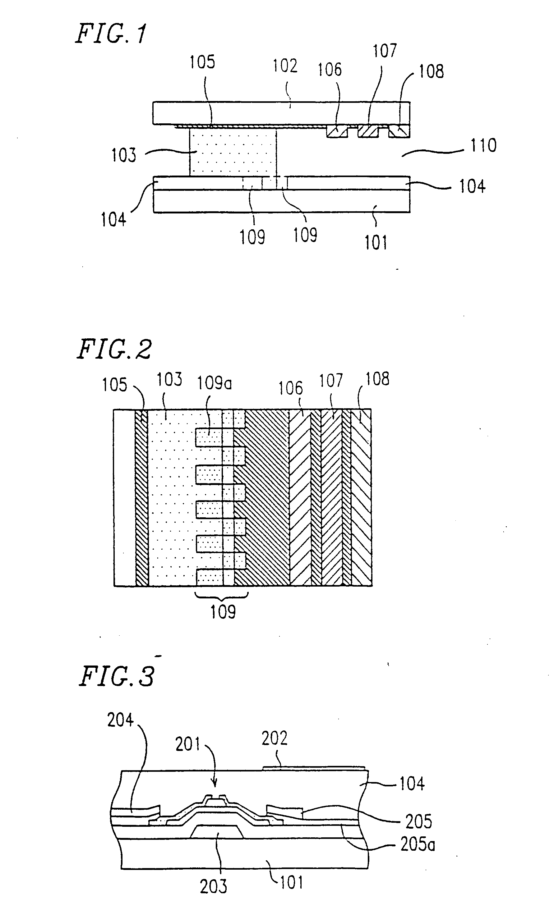
[0097]FIG. 1 is a schematic cross-sectional view showing the vicinity of the sealing material of a liquid crystal display device according to a preferred embodiment of the present invention, and FIG. 2 is a schematic plan view of the liquid crystal display device. FIG. 3 is a schematic cross-sectional view showing the TFT portion of the liquid crystal display device.

[0098] The liquid crystal display device comprises a TFT substrate 101 and a color filter substrate 102 both of which are opposite to each other, and a sealing material 103 formed in the periphery portion between the substrates 101 and 102. Preferably, the sealing material 103 is continuously formed on the four sides of the periphery portion. A liquid crystal layer 110 is interposed between the substrates 101 and 102 and is sealed by the sealing material 103. The liquid crystal layer may contain any suitable liquid crystal material. The substrates 101 and 102 are disposed at the prescribed cell gap by using an intra-sea...

embodiment 2

[0123] This embodiment provides a case where a black matrix 301 of the color filter substrate 102 is made from the same resin material as that of the color layers 106, 107 and 108, as illustrated in FIG. 12. The outflow preventing portion 109 is formed in the interlayer insulating film 104 of the TFT substrate 101 as with Embodiment 1.

[0124] In this case, since the black matrix is formed from a resin material, it is possible to increase the thickness of the black matrix 301. For example, the thickness of the black matrix is about 15000 angstroms in this embodiment. Therefore, it is possible to flatten the surface of the color filter. When a black matrix made from a resin material is used, the cell gap of the liquid crystal layer portion will be substantially equal to that of the sealing portion, unlike a case of using a black matrix made from a metal (for example, Cr). Thus, a difference in level between the black matrix 105 made from Cr (i.e., not made from a resin) and the color ...

embodiment 3

[0132] The following illustrates an active-matrix-type liquid crystal display device which is still another embodiment of the present invention. First, the circuit of the active matrix-type liquid crystal display device is illustrated with reference to FIG. 14. Gate bus lines 4 which are scanning lines are connected to a plurality of scanning terminals 2 located in the linear direction, while source bus lines 8 which are signal lines are connected to a plurality of signal terminals 6 located in the row direction. Each of the gate bus lines 4 and each of the source bus lines 8 cross each other (substantially at a right angle in this embodiment). A display pixel 10 is formed in a region surrounded by the adjacent gate bus lines and the adjacent source bus lines. The display pixel 10 comprises a pixel electrode 12, a switching element (an active element) 14 such as TFT, and a storage capacitor 16. The pixel electrode 12 is opposite to a counter electrode 18. The storage capacitor 16 is...


PUM

PropertyMeasurementUnit
diameteraaaaaaaaaa
particle sizeaaaaaaaaaa
thicknessaaaaaaaaaa

Abstract

A liquid crystal display device includes a pair of opposed substrates, and a liquid crystal layer as a display medium disposed between said substrates. The pair of substrates are adhered together by a resin sealing material disposed on the periphery portion of at least one of the substrates at a prescribed gap, and an outflow preventing portion is provided.

Description

BACKGROUND OF THE INVENTION [0001] 1. Field of the Invention [0002] The present invention relates to a liquid crystal display device and a process for producing the same. In particular, the present invention relates to a liquid crystal display device having excellent mechanical strength as well as sealing property without any poor display caused by a sealing material, and a process for producing the same. [0003] 2. Description of the Related Art [0004] A liquid crystal display device comprises a pair of insulating substrates (typically, glass substrates) 101 and 102, and a liquid crystal layer 110 as a display medium which is disposed between the substrates, as illustrated in FIG. 36. On the glass substrate 101, an active element (typically, thin film transistor (TFT)) which controls the electro-optical characteristics of the liquid crystal, and a scanning line and a signal line which give a gate signal and a source signal, respectively, to the active element are provided. This subs...

Claims


Application Information

Patent Timeline
Patent Type & Authority Applications(United States)
IPC IPC(8): G02F1/1339
CPCG02F1/1339G02F1/136
Inventor FUJIOKA, KAZUYOSHINARUTAKI, YOZONAGATA, HISASHIMIYAMOTO, KAZUSHIGESHIMADA, TAKAYUKI
Owner SHARP KK
Why Eureka
Try Eureka