
Method and apparatus for self-assembly of functional blocks on a substrate facilitated by electrode pairs

a functional block and electrode pair technology, applied in the field of self-assembly and mounting, can solve the problems of high material and processing cost, inability to make large-area flat-panel displays cost effectively from single-crystal-silicon substrates, and inability to meet the needs of large-area flat-panel displays, etc., to achieve high magnetic permeability and high magnetic

Inactive Publication Date: 2005-01-13
RUIZHANG TECH LTD CO
View PDF28 Cites 42 Cited by
  • Summary
  • Abstract
  • Description
  • Claims
  • Application Information

AI Technical Summary

Benefits of technology

"The patent describes methods and apparatuses for attracting, aligning, and securing functional blocks on a substrate using electric and magnetic forces. The technical effects include the ability to attract and guide functional blocks to specific locations on a substrate, as well as the ability to clean excess functional blocks from the substrate."

Problems solved by technology

The high cost of materials and processing must be divided among many, small functional blocks.
Unfortunately, different materials can require different processing, and these materials and processes are not often compatible.
As an example of how an improved self-assembly process can be beneficially applied to the first case, large area flat panel displays cannot be made cost effectively from single-crystal-silicon substrates.
However, it is cost effective to construct large displays by mounting small, single-crystal-silicon transistors on low cost substrates.
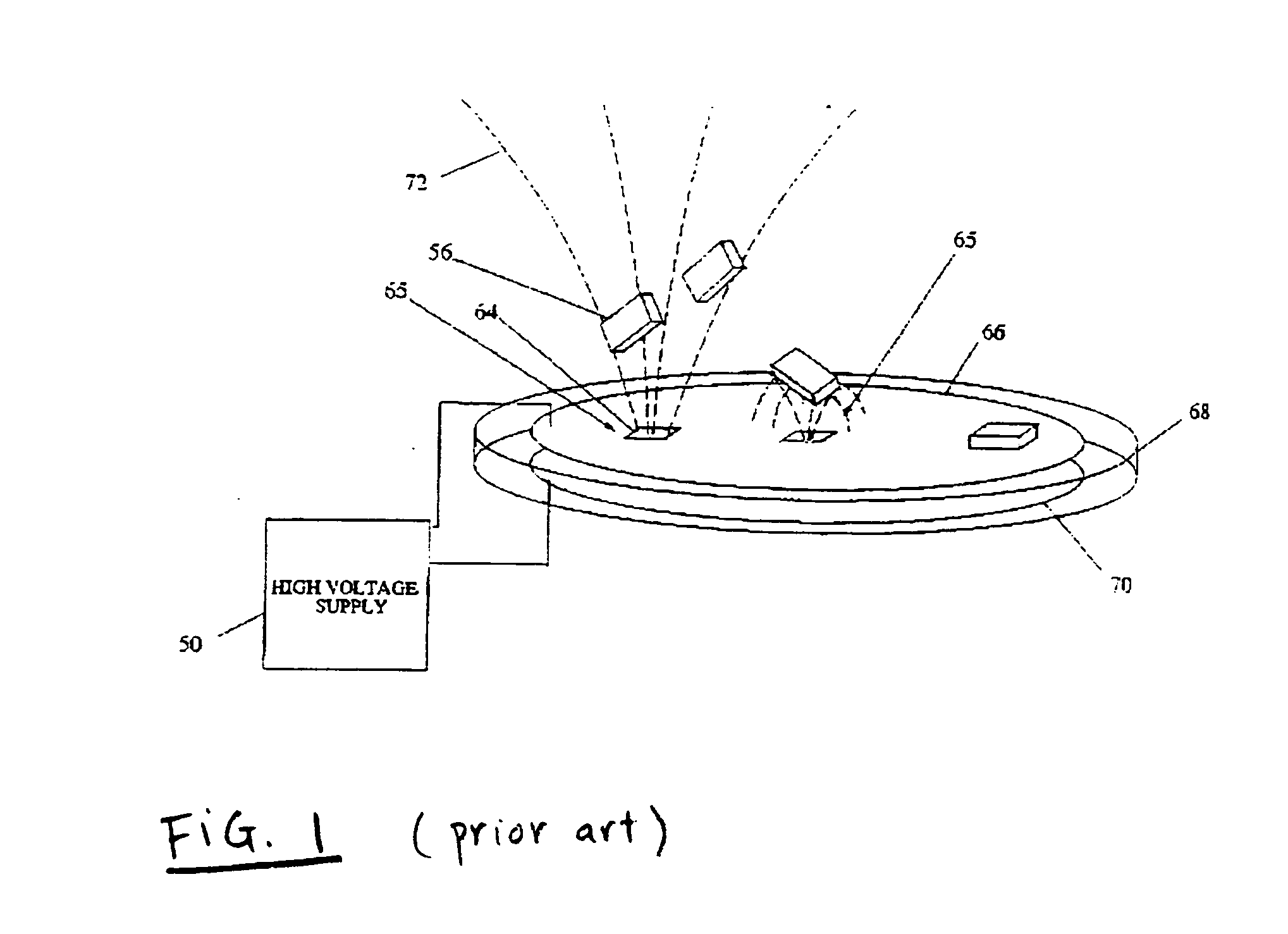
However, severe limitations exist on the shape, size, and distribution of the functional blocks.
In addition, self-alignment of functional blocks requires the presence of the laminated magnetic structure which puts severe limitations on the materials that can be used for both the substrate and functional blocks and can result in higher material cost.
Furthermore, the structures disclosed by Yando typically possess millimeter sized dimensions and are therefore generally incompatible with micron sized integrated circuit structures.
Accordingly, the method and structure disclosed by Yando is thereby too large and complicated to be effective for assembling a state-of-art microstructure of functional blocks onto a substrate.
Such a process is limiting because of the need for a human or robotic arm.
The human or robotic arm assembles each packaged device onto a substrate in a serial fashion, one device at a time and not simultaneously, thereby limiting the rate, efficiency, and effectiveness of the operation.
Moreover, the method uses centimeter sized devices (or packaged surface mount integrated circuits), and would have little applicability with micron sized integrated circuits in die form.
Moreover, the method described relies upon centimeter-sized die and would have little applicability with state-of-art micron sized structures.
The method becomes limiting because of the need for a shaking apparatus for the electromagnetic shaking step.
Moreover, the method is solely in context to electrode pedestals and silicon wafers, thereby limiting the use of such method to those structures.
Second, it is unlikely that the extensive electrodes used for trapping will be compatible with most finished products, hence additional process steps must be added to remove these electrodes after trapping.
Further, once the trapping electrodes are removed, the trapping process cannot be reworked, repeated, without reforming the electrodes.
And if the possibility of rework is to be allowed, then the trapping electrodes cannot also be used as electrical interconnects between devices, as the high trapping voltage recommended, ˜8 kV, is not compatible with microelectronic functional blocks.
An additional limitation resulting from use of parallel-plate electrodes, which substantially cover the substrate, is that there is no easy, electrical means of determining when all trapping sites are occupied.
Hence the change in electrical characteristics is too small to detect.
A further limitation resulting from use of electrodes which substantially cover a substrate and use of the suggested high trapping voltage is that a majority of the substrate is subjected to very high electric field strength, greatly increasing the odds of failure due to dielectric breakdown.
Hence the substrate material and construction must be of a universally high quality, with resulting higher costs.
Further, the high bias voltage presented is not compatible with materials of this thickness.
The reason alignment fails is that, during mounting, devices are not ohmically connected to the top electrode, but rather are capacitively coupled.
Cohn does not discuss the type of electrical connection in the 5,355,577 patent, but given the small size of devices envisioned, and the weak forces employed, achieving an ohmic connection is not tenable.
However, a limitation exists during mounting in that functional blocks must have a lower average dielectric constant than that of the surrounding medium.
Furthermore, the required electrode configuration is complex and must cover the entire substrate surface.
Hence all the limitations discussed above regarding “electrodes that substantially cover the substrate” still apply here, plus limitations regarding the additional complexity of the electrode configuration.
Even with the techniques above, the concentration of functional blocks upon regions of receptor sites is not good enough.
Thus, it is difficult to control the incident of the functional blocks upon the receptor sites.

Method used


Image

  • Method and apparatus for self-assembly of functional blocks on a substrate facilitated by electrode pairs
  • Method and apparatus for self-assembly of functional blocks on a substrate facilitated by electrode pairs
  • Method and apparatus for self-assembly of functional blocks on a substrate facilitated by electrode pairs

Examples


Embodiment Construction

Theory of Operation

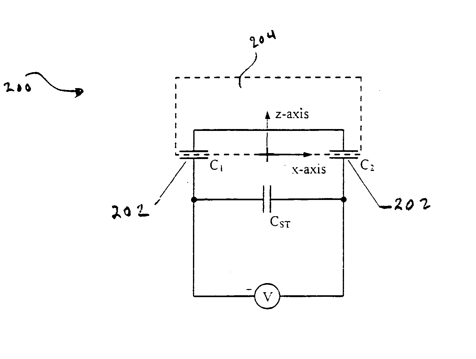
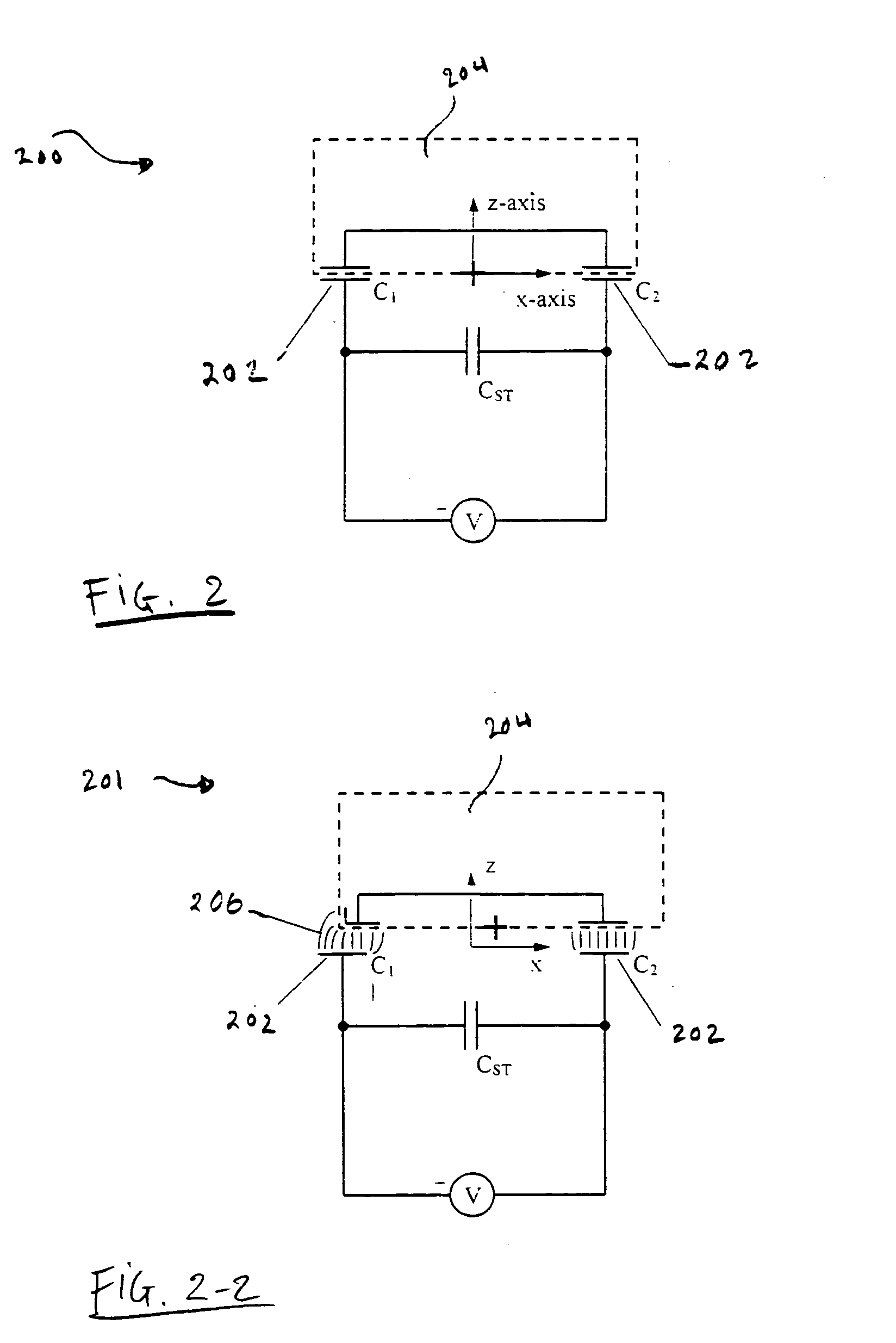
The present invention relies on electrostatic forces generated between sets (usually pairs) of substrate bound mounting-electrodes and functional blocks. The planar electrostatic chunk geometry employed in this invention produce local electrostatic forces within a functional block that are a function of the difference between the local dielectric constant in the functional block and the dielectric constant of the medium surrounding the functional blocks during the assembling or mounting procedure. These forces include dielectrophoresis and negative-dielectrophoresis. Hence the distribution of materials (i.e., of different dielectric constant) within a functional block and the geometry of the mounting-electrodes determine the forces and torques acting on a functional block at a given location. The force or torque acting on a functional block at a given location is equal to the change of energy in the electrostatic field,

U=f(½)k·εO·E2dv  (equation 1),

for a sma...


PUM


Abstract

Methods for fabricating an assembly having functional blocks coupling to a substrate. The method includes providing the substrate with receptor sites wherein each of the receptor sites is designed to couple to one of the functional blocks. Electrodes are coupled to the substrate. The electrodes cover the receptor sites such that portions of the receptor sites are coated with the electrodes. Applying a voltage source to the electrodes using a first electrical circuit such that each electrode has a voltage different from another electrode. The electrodes form an electric field. The functional blocks having electronic devices and being in a slurry solution are dispensed over the substrate. Each functional block is fabricated out of materials having a high dielectric constant such that said functional blocks are attracted to the higher field strength regions and are guided to the receptor sites.

Description

FIELD OF THE INVENTION The invention relates to the fields of electronics, integrated circuits, opto-electronics, and assemblies of functional blocks, and specifically to the self-assembly and mounting of these small functional blocks onto a substrate to form larger, compound electronic or opto-electronic assemblies. BACKGROUND OF THE INVENTION There is a pressing need for new techniques of self-assembling small functional blocks onto a substrate. Two main factors drive this need. First, the economic of integrated circuit (IC) manufacturing is that of an economy of scale. The high cost of materials and processing must be divided among many, small functional blocks. Second, optimum device performance often requires that different functions of a device be performed by different materials, each possessing unique properties. Unfortunately, different materials can require different processing, and these materials and processes are not often compatible. Hence elements that make up a dev...

Claims


Application Information

Patent Timeline
Patent Type & Authority Applications(United States)
IPC IPC(8): H01L21/98
CPCH01L24/95H01L25/50H01L2924/12044H01L2924/12042Y10T428/24917H01L2924/15787H01L2924/12041H01L2224/83894H01L2224/95085H01L2224/95122H01L2224/95136H01L2224/95144H01L2224/95145H01L2924/01013H01L2924/01015H01L2924/01027H01L2924/01039H01L2924/01078H01L2924/09701H01L2924/10158H01L2924/14H01L2924/15153H01L2924/15165H01L2924/19041H01L2924/30105H01L2924/01005H01L2924/01019H01L2924/01023H01L2924/01033H01L2924/00
Inventor SCHATZ, KENNETH DAVID
Owner RUIZHANG TECH LTD CO
Learn More