Adaptive correlation of pattern resist structures using optical metrology

a pattern resist and optical metrology technology, applied in the field of integrated circuit (ic) metrology, can solve the problems of high cost of cd-sem and the need to be employed in a vacuum environment, and achieve the effect of improving the photolithographic process

Active Publication Date: 2005-01-13
TOKYO ELECTRON LTD
View PDF5 Cites 23 Cited by
  • Summary
  • Abstract
  • Description
  • Claims
  • Application Information

AI Technical Summary

Problems solved by technology

However, CD-SEM is costly and must be employed in a vacuum environment.

Method used


Image

  • Adaptive correlation of pattern resist structures using optical metrology
  • Adaptive correlation of pattern resist structures using optical metrology
  • Adaptive correlation of pattern resist structures using optical metrology

Examples


Embodiment Construction

The following description is presented to enable one of ordinary skill in the art to make and use the invention and is provided in the context of a patent application and its requirements. In the following description, specific nomenclature is set forth to provide a thorough understanding of the present invention. It will be apparent to one skilled in the art that the specific details may not be necessary to practice the present invention. Furthermore, various modifications to the embodiments will be readily apparent to those skilled in the art and the generic principles herein may be applied to other embodiments. Thus, the present invention is not intended to be limited to the embodiments shown but is to be accorded the widest scope consistent with the principles and features described herein.

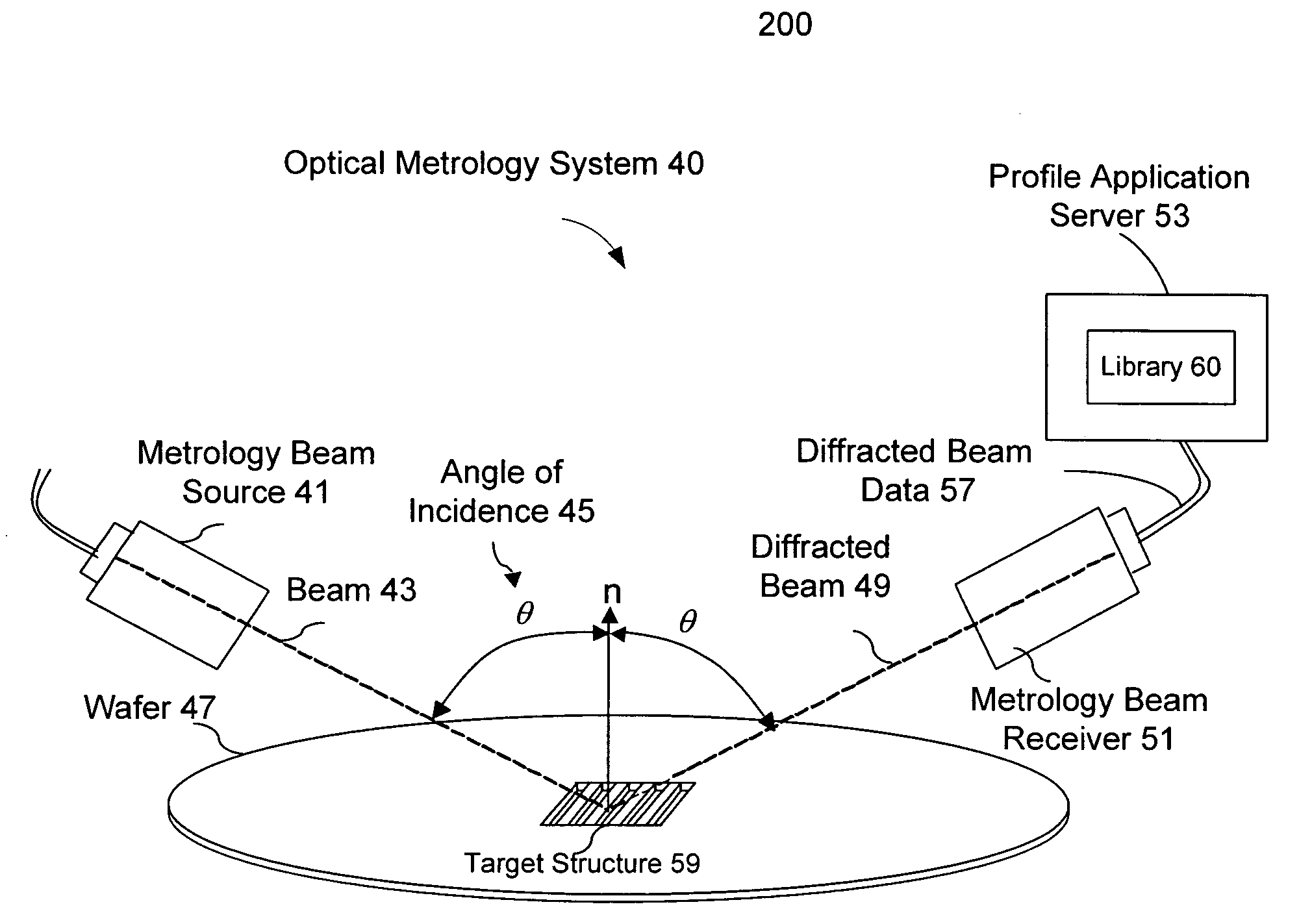
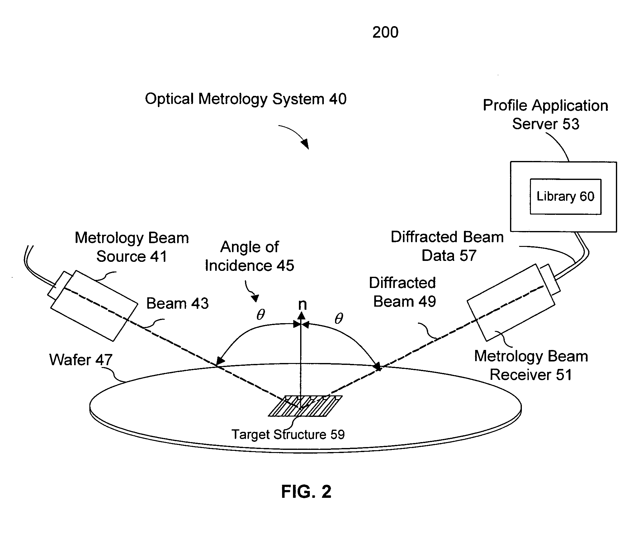
In order to facilitate the description of the present invention, an ellipsometric optical metrology system is used to illustrate the concepts and principles. It is understood that the same ...


PUM


Abstract

A correlation between develop inspect (DI) and final inspect (FI) profile parameters are established empirically with test wafers. During production, a wafer is measured at DI phase to obtain DI profile parameters and FI phase profile parameters are predicted according to the DI profile parameters and the established correlation. Each wafer is subsequently measured at FI phase to obtain actual FI profile parameters and the correlation is updated with actual DI and FI profile parameters.

Description

BACKGROUND 1. Field of the Invention The invention relates to integrated circuit (IC) metrology and more particularly to a method and system for quality monitoring of photolithography processing. 2. Related Art Growing demands for silicon wafers with large-scale integration necessitates submicron integrated circuit (IC) features with high precision and uniformity. As the features become smaller, it is increasingly critical to monitor the photolithographic process under which such semiconductor wafers are created. In a typical photolithographic process, a series of masks are applied in a preset sequence to a silicon wafer, each mask is used to transfer its circuitry pattern onto a photosensitive layer (i.e., a photoresist layer) that is coated onto a layer (e.g., metal layer, etc.) formed on the silicon wafer. FIG. 1 is a flow chart 100 illustrating conventional process steps for transferring a circuitry pattern from a mask to a silicon wafer. A silicon wafer is coated with phot...

Claims


Application Information

Patent Timeline
Patent Type & Authority Applications(United States)
IPC IPC(8): H01L21/00
CPCG05B2219/32368H01L21/67276G05B2219/45031Y02P90/02
Inventor ENGELHARD, DANIEL EDWARDMADRIAGA, MANUEL B.
Owner TOKYO ELECTRON LTD
Why Eureka
Try Eureka