Level shift circuit

a level shift circuit and level shift technology, applied in logic circuits, logic circuit coupling/interface arrangements, pulse techniques, etc., can solve the problems of deteriorating operation speed of the level shift circuit as a whole, and become conspicuous, so as to improve the current driving capability of the inverted output node and the change to the h level of the output node, the operation speed of the level shift circuit is increased, and the speed of the inverted output node and the inverted output no

Inactive Publication Date: 2005-01-13
SOCIONEXT INC
View PDF10 Cites 6 Cited by
  • Summary
  • Abstract
  • Description
  • Claims
  • Application Information

AI Technical Summary

Benefits of technology

In addition, in the invention, for example, when the input signal of the input terminal changes from the L level to the H level, the first N-type transistor is made conducting, current flows in the transistor, and the current is amplified by predetermined number of times by the first current mirror circuit. Further, a first N-type current feedback transistor and an N-type transistor as a component of the N-type current mirror of the first current mirror circuit construct another current mirror circuit. The another current mirror circuit amplifies the amplified current. The amplified current is amplified again by the first current mirror circuit. The operation is repeated, and the amplified current is drawn out from the inverted output node. Therefore, the current driving capability for the inverted output node remarkably improves. The speed of the change to the L level of the inverted output node and the change to the H level of the output node is increased, and the operation speed of the level shift circuit increases.
Particularly, in the invention, for example, when the input signal of the input terminal is at the L level, inherently, current does not flow in the first current mirror circuit. When the amount of leak current is large, the current mirror circuit including the first N-type current feedback transistor amplifies the leak current, and the inverted input signal of the inverted input terminal tends to become the L level erroneously. The third N-type transistor leads the leak current to the ground, so that such erroneous operation can be prevented.
In the invention, in a stationary state in which the input signal maintains the H level after the first current mirror circuit amplifies the current by the predetermined number of times as described above, the first current mirror circuit always passes the current amplified by the predetermined number of times. However, after the change to the H level of the output signal of the output node is finished, the first current interrupting circuit operates to interrupt the amplified current fed from the first current mirror circuit. Thus, power consumption can be effectively reduced.
Further, in the invention, for example, when the output signal changes from the L level to the H level at the output node, the second change speed accelerating circuit accelerates the speed of the change to the H level of the output signal, so that the operation speed further improves.
In addition, in the invention, in the initial state where the power source starts to be supplied, even in the case where the input signal and the inverted input signal of the input terminal and the inverted input terminal are not at the predetermined L or H level but are indeterminate, the stabilizing circuit operates to determine the potential of each of the output node and the inverted output node to the L or H level early and stabilize it. Consequently, transient current which flows until the stable state is obtained can be effectively reduced.

Problems solved by technology

It was, however, found that when the power source voltage decreases more in the conventional level shift circuit, the following problems become conspicuous.
As a result, when the signals IN and XIN change from 0V to the predetermined voltage level (0.7V), the operation of the N-type transistors 1 and 2 on the side of shifting to the conducting state is slow, and a problem occurs such that the operation speed of the level shift circuit as a whole deteriorates.
Consequently, as the level of the voltage further decreases, it is becoming an important issue to shift a signal of the low voltage level to a signal of the high voltage level at speed as high as possible.

Method used


Image

  • Level shift circuit
  • Level shift circuit
  • Level shift circuit

Examples


embodiment 1

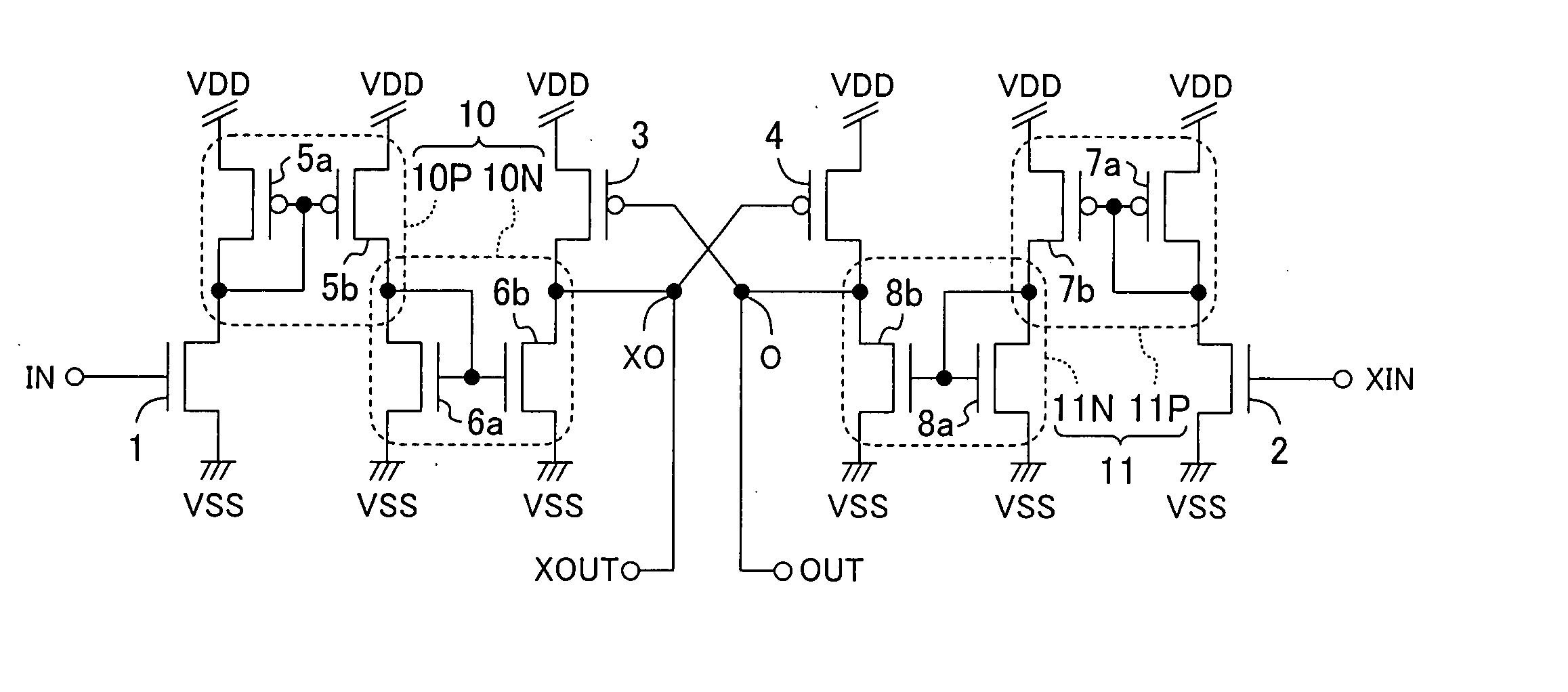
FIG. 1 shows a level shift circuit of a first embodiment of the invention.

Shown in the diagram are a high voltage power source VDD, a ground power source VSS, an input terminal IN, an inverted input terminal XIN, an output node O, an inverted output node XO, an output terminal OUT connected to the output node O, and an inverted output terminal XOUT connected to the inverted output node XO. It is not always necessary to provide a pair of the output terminal OUT and the inverted output terminal XOUT. It is sufficient to provide either the terminal OUT or XOUT as necessary.

Reference numeral 1 denotes a first N-type signal input transistor and an input signal (to which the same reference characters “IN” as those of the input terminal IN are designated) of the input terminal IN is input to the gate electrode of the first N-type transistor 1. Reference numeral 2 denotes a second N-type signal input transistor and an inverted input signal (to which the same reference characters “XIN” a...

embodiment 2

FIG. 3 shows a level shift circuit of a second embodiment of the invention.

The level shift circuit of the diagram is obtained by improving the level shift circuit of the first embodiment to reduce the current steadily flowing in the first and second current mirror circuits 10 and 11.

Specifically, the level shift circuit of FIG. 3 is obtained by adding two P-type transistors 15 and 16 to the configuration of the level shift circuit of the first embodiment. In the P-type transistor 15, the source electrode is connected to the high voltage source VDD, the drain electrode is connected to the P-type current mirror circuit 10P in the first current mirror circuit 10, and the gate electrode is connected to the output node O and receives the output signal O. Similarly, in the other P-type transistor 16, the source electrode is connected to the high voltage source VDD, the drain electrode is connected to the P-type current mirror circuit 11P of the second current mirror circuit 11, and th...

embodiment 3

FIG. 8 shows a level shift circuit of a third embodiment of the invention.

The level shift circuit of FIG. 8 is obtained by further improving the level shift circuit of the second embodiment shown in FIG. 3. Specifically, the level shift circuit of FIG. 8 is obtained by adding first and second change speed accelerating circuits 20 and 21 to the level shift circuit of FIG. 3. The first and second change speed accelerating circuits 20 and 21 are to accelerate change speed from the L level to the H level of the inverted output node XO and the output node O as will be described later.

The first change speed accelerating circuit 20 includes a first P-type transistor 30 connected in parallel with the P-type transistor 5a on the input side as a component of the P-type current mirror circuit 10P of the first current mirror circuit 10, and a first buffer circuit 33 constructed by two inverter circuits 31 and 32. The first P-type transistor 30 is set to have a large gate width and extremely...


PUM


Abstract

In a level shift circuit, for example, when an input signal IN changes from the L level to the H level, an N-type signal input transistor is made conducting and current flows in the N-type transistor. Accordingly, a first current mirror circuit amplifies the current flowing in the N-type transistor by predetermined number of times, increases the current driving capability for an inverted output node, and changes the inverted output node quickly to the L level. With the change to the L level of the inverted output node, an output node changes to the H level, a P-type transistor (first current interrupting circuit) is made non-conducting by the change, and the current fed from the first current mirror circuit is interrupted. Therefore, even when the power source voltage for the input signal and the inverted input signal is lowered, the operation is performed at high speed.

Description

BACKGROUND OF THE INVENTION The present invention relates to a level shift circuit used for an interface between circuits with different power source voltages. As processing is becoming finer in recent years, there has been a tendency toward reducing the power source voltage of circuits in semiconductor integrated circuits for the sake of device reliability. On the other hand, devices used in a system such as electronic equipment include a device operated on the conventional power source voltage. To interface between the devices and the semiconductor integrated circuit using different power source voltages, generally, a level shift circuit is provided in the semiconductor integrated circuit. Recently, also in a semiconductor integrated circuit, an optimum power source voltage is supplied to each of circuit blocks in order to reduce power consumption. To interface among the circuit blocks of different power source voltages, a level shift circuit is also used. It is expected that i...

Claims


Application Information

Patent Timeline
Patent Type & Authority Applications(United States)
IPC IPC(8): H03K3/356
CPCH03K3/356113
Inventor GION, MASAHIRO
Owner SOCIONEXT INC
Why Eureka
Try Eureka