
Method and system of lithography using masks having gray-tone features

a technology of masks and graytones, applied in the field of fabrication methods, can solve the problems of limited resolution of optical steppers, high cost of lenses with very high numerical apertures ("na") approaching 0.9 to 1.0, and further limited

Inactive Publication Date: 2004-12-23
MASSACHUSETTS INST OF TECH
View PDF9 Cites 32 Cited by
  • Summary
  • Abstract
  • Description
  • Claims
  • Application Information

AI Technical Summary

Problems solved by technology

However, the resolution of an optical stepper is limited by the wavelength of the light source, and is further limited by the numerical aperture ("NA") of the lens.
In this field, the cost of lenses having very high numerical apertures ("NA") approaching 0.9 to 1.0 is very high.
Moreover, linear NA increases are not sufficient to maintain pace with the need for exponentially decreasing feature sizes.
However, the conventional RET methods face problems of layout complexity and data size, mask fabrication complexity and resulting cost, and optical proximity and spatial frequency effects which are discussed below.
Moreover, optical proximity effects can become more severe in sub-wavelength lithography.
Since the performance of the circuit depends on the size and size tolerance of the gates, this is an undesirable result.
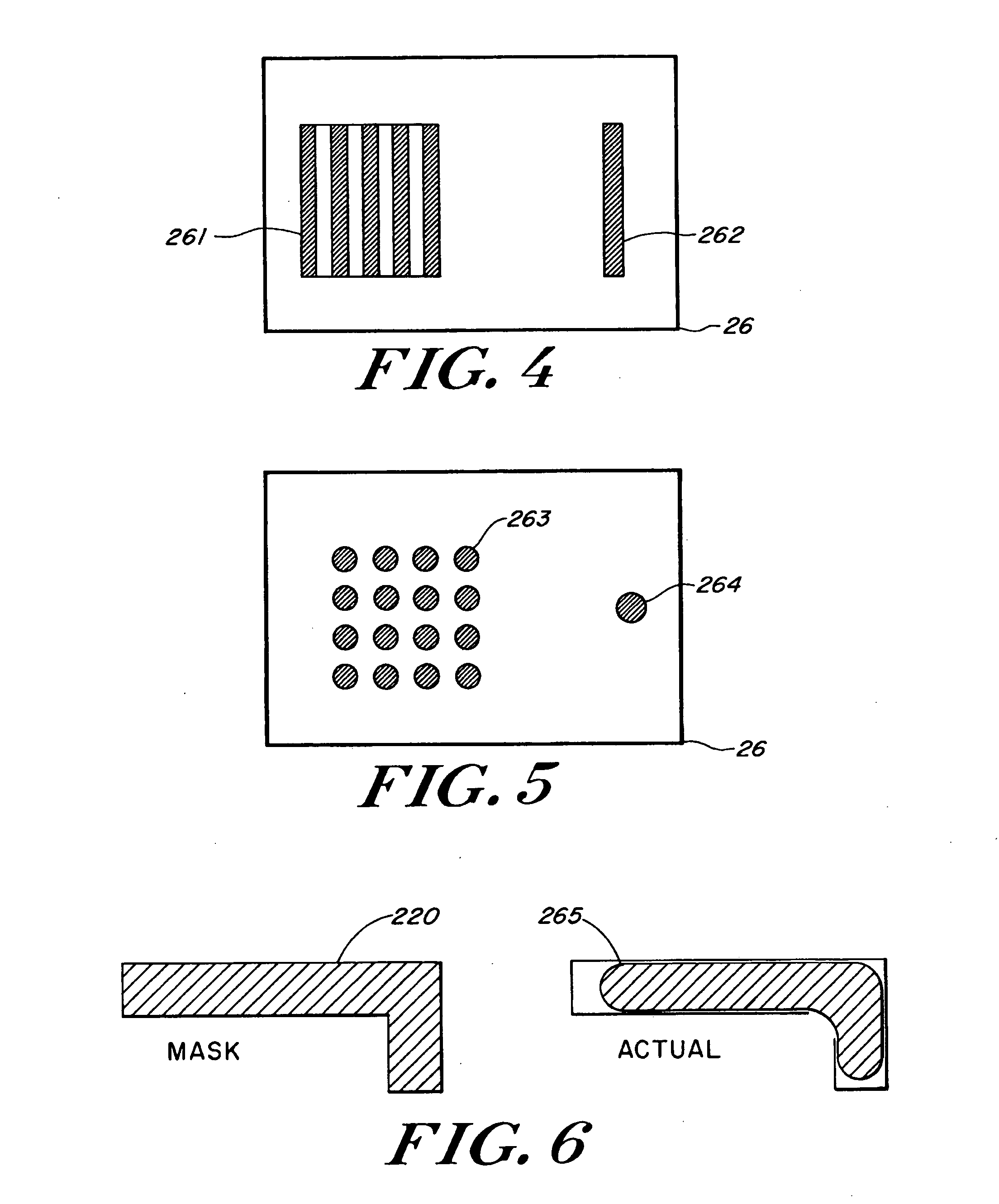
This results in corner rounding and line end shortening.
For this reason, conventional feature size correction ("OPC" or optical proximity correction) is a costly and time-consuming process.
The hierarchical data processing algorithms used for conventional circuit design are of limited utility because optical proximity effects are based on the nature of geometries surrounding a particular circuit element.
Brueck et al. does not address optical proximity and spatial frequency effect problems thus limiting the ultimate density and flexibility of the patterns produced.
In addition, the multiple exposures are not substantially independent in the optical sense due to the resist's "memory" of previous exposure patterns.
It is also difficult to make an arbitrary two-dimensional pattern in this way.
Suzuki et al. does not address optical proximity and spatial frequency effect problems thus limiting the ultimate density and flexibility of the patterns produced.
It is also difficult to realize an arbitrary 2D pattern with this method.
Since the fine features are only realized in one orientation, it is difficult to form patterns with fine features in both the x & y directions.
Just as in the previous Patents discussed above, this method does not mitigate optical proximity and spatial frequency effects.
This process addresses the spatial frequency effect problems of corner rounding and line-end shortening, but does not resolve the optical proximity effect problem.
One of the challenges of this approach is the imaging of a variety of near minimum width feature sizes, by varying widths of chrome regulator features at each phase transition.
As feature sizes continue to scale into the deep sub-wavelength regime, it becomes more difficult to fabricate multiple sizes of critical dimension features by varying chrome regulator width.
In addition, state of the art chromeless phase shift lithography methods, which are capable of the largest resolution enhancement, cannot be used to image multiple fine feature critical dimensions in a single die.
As feature sizes continue to move ever deeper into the sub-wavelength regime, it becomes increasingly difficult to image a variety of critical dimensions using this method.
In addition, chromeless phase shift masks, which have great resolution enhancement potential, cannot be used to image multiple critical dimensions
This is especially desirable since conventional optical proximity correction approaches are becoming quite difficult to implement as imaging requirements continue to move deeper into the sub-wavelength regime.

Method used


Image

  • Method and system of lithography using masks having gray-tone features
  • Method and system of lithography using masks having gray-tone features
  • Method and system of lithography using masks having gray-tone features

Examples


Embodiment Construction

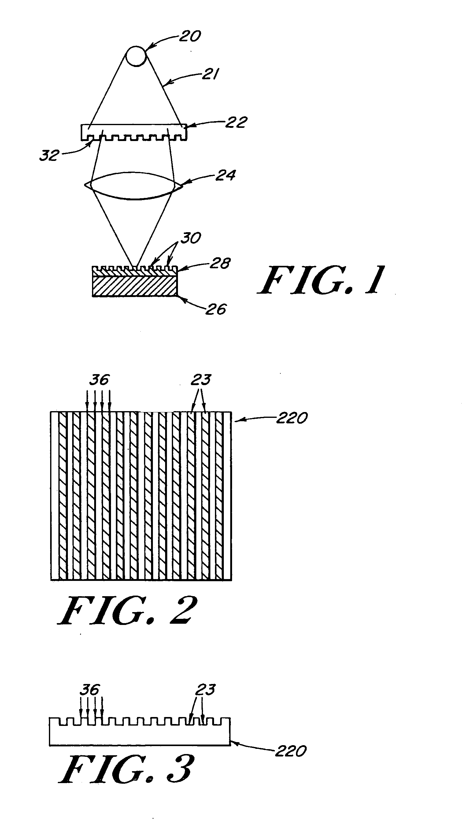
[0079] The present invention is directed to an imaging approach that overcomes the limitations of the conventional techniques, and confers a number of advantages. It addresses the problems of optical proximity and spatial frequency effects while maintaining the resolution-enhancement performance required by sub-wavelength lithography. Moreover, the present invention addresses the problems associated with lithographically defining features with locally variable critical dimension. The present invention also provides local control of the effective exposure dose that defines the critical dimension of the feature so that a wide variety of small features can be imaged without the need for chrome regulators or additional exposures.

[0080] In the following description, the phrase, "lines," refers to either the trenches or the raised areas; e.g., plateaus; on a wafer. Moreover, the phrase, "contacts," refers to either the holes or pillars on a wafer. The described photoresists may either be ...


PUM

PropertyMeasurementUnit
wavelengthaaaaaaaaaa
optical simulationaaaaaaaaaa
widthaaaaaaaaaa

Abstract

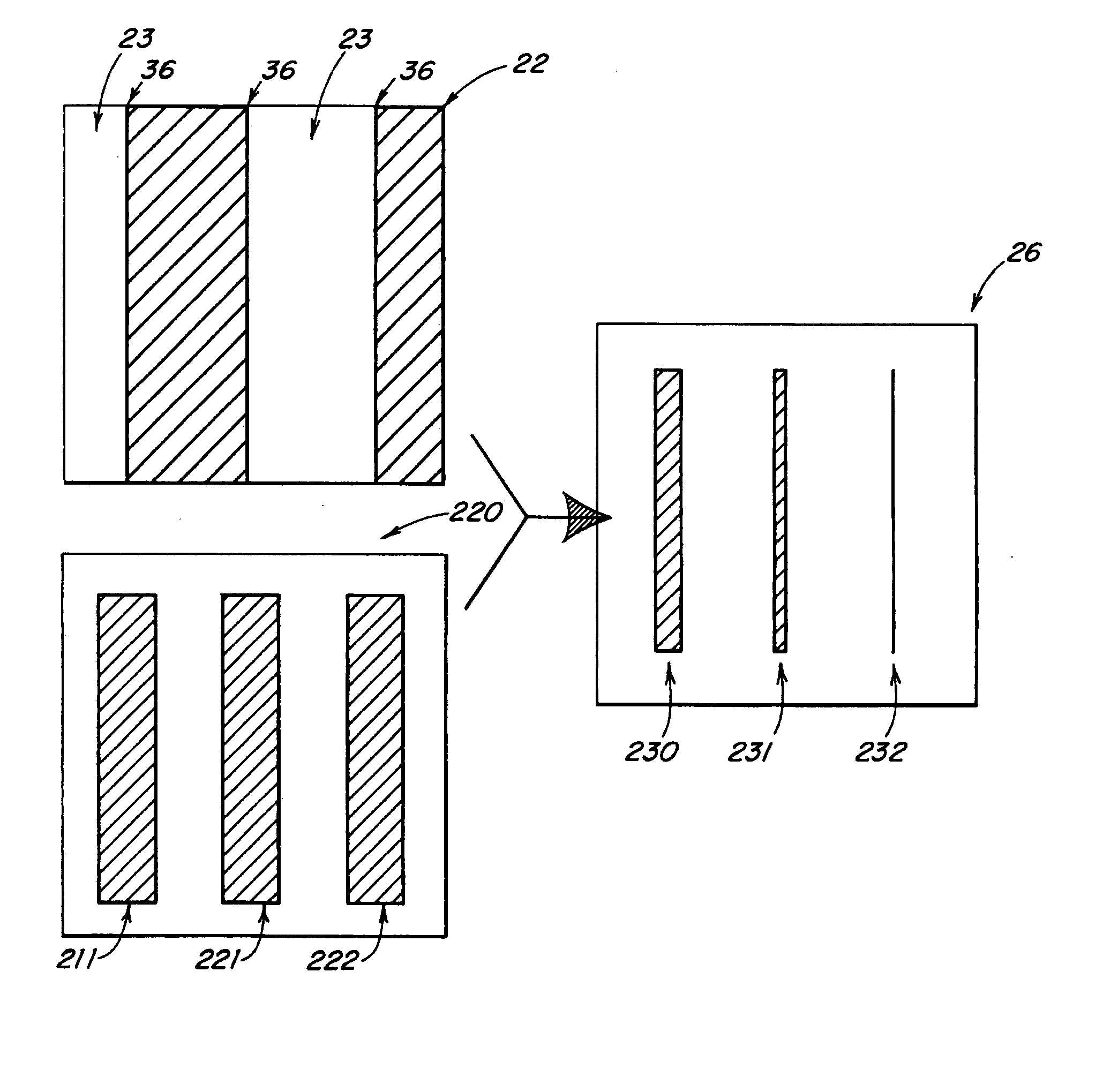
A method forms patterns on a substrate by exposing the substrate a first time and exposing the substrate a second time using a mask containing gray-tone features. The gray-tone features locally adjust an exposure dose in regions corresponding to features defined in the primary exposure. Moreover, the gray-tone features enable the forming of features having different critical dimensions on a substrate. The gray-tone features may be sub-resolution features and formed by pixellation. The trim mask containing gray-tone features may have regions with different transmissivities.

Description

CROSS-REFERENCE TO RELATED PROVISIONAL APPLICATION[0001] The present patent application claims priority under 35 U.S.C. .sctn. 119 from U.S. Provisional Patent Application Ser. No. 60 / 361,612 filed on Mar. 4, 2002. The entire contents of U.S. Provisional Patent Application Ser. No. 60 / 361,612 filed on Mar. 4, 2002 are hereby incorporated by reference.FIELD OF THE PRESENT INVENTION[0002] The present invention is directed to fabrication methods, such as double exposure lithography, which initially form a pattern on a substrate and then trims the formed pattern. More particularly, the present invention is directed to a process and methodology of controlling feature critical dimension using gray-tone mask features.BACKGROUND OF THE PRESENT INVENTION[0003] Conventional optical projection lithography has been the standard silicon patterning technology for the past 20 years. It is an economical process due to its inherently high throughput, thereby providing a desirable low cost per part o...

Claims


Application Information

Patent Timeline
Patent Type & Authority Applications(United States)
IPC IPC(8): G03F1/00G03F7/00G03F7/20
CPCB82Y10/00B82Y40/00G03F1/144G03F7/0002G03F7/2022G03F7/70283G03F1/50G03F1/70
Inventor FRITZE, MICHAELTYRRELL, BRIAN
Owner MASSACHUSETTS INST OF TECH
Learn More