Circuit board, circuit board mounting method, and electronic device using the circuit board
a technology of circuit board and mounting method, applied in the direction of printed element electric connection formation, printed circuit non-printed electric component association, final product manufacture, etc., can solve the problem of significant decrease in reliability of electronic equipmen
- Summary
- Abstract
- Description
- Claims
- Application Information
AI Technical Summary
Benefits of technology
Problems solved by technology
Method used
Image

Examples
embodiment 1
[0078] [Embodiment 1]
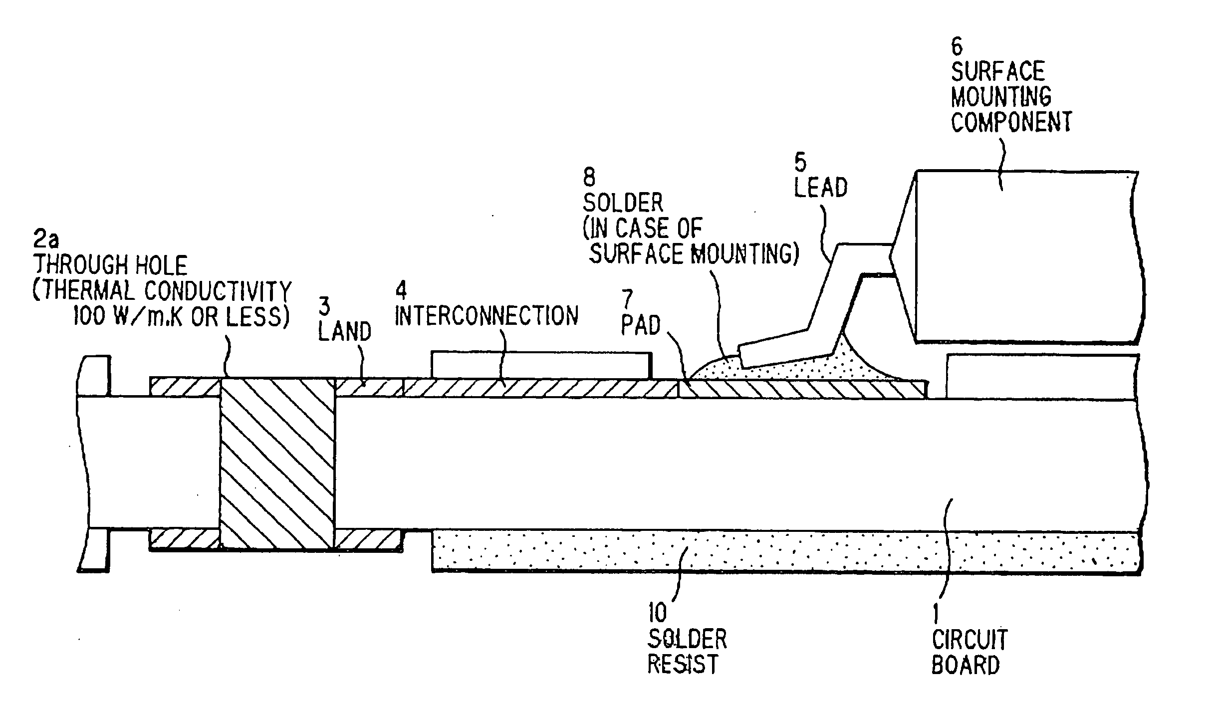
[0079] As shown in FIGS. 5 through 12, a circuit board according to the first embodiment of the present invention is constituted in such that at least one member selected from an inner wall of a through hole to be defined in the circuit board, a land of the through hole, and a material to be filled inside the through hole is composed of the one having a thermal conductivity equal to or lower than a predetermined value, whereby conduction of heat transmitted via the through hole in case of wave-soldering is suppressed. A material having a low thermal conductivity is disposed on a heat conductive path, so that heat flows into solder in a lead joined site in a surface mounting component through an interconnection thereby preventing melting of a alloy layer formed in the lead joined site.
[0080] In this case, it is the better that a material of the inner wall of the through hole, that of the land, or that to be filled inside the through hole has the lower thermal con...
embodiment 2
[0081] [Embodiment 2]
[0082] As shown in FIGS. 13 through 26, a circuit board according to the second embodiment of the present invention is constituted in such that at least a part of an interconnection between a through hole defined in the circuit board and a pad to which a lead of a surface mounting component is to be joined is composed of a material having a thermal conductivity equal to or lower than a predetermined value, or an interconnection length is made to be a value equal to or longer than a predetermined value, or further an sectional area of the interconnection is made to be equal to or lower than a predetermined value. Thus, thermal conduction transmitted via the through hole at the time of wave-soldering is suppressed, so that heat flowing into solder in a lead joined site of the surface mounting component transmitted through the interconnection is suppressed, whereby fusion of a alloy layer formed in the lead joined site is prevented.
[0083] It is preferred herein tha...
embodiment 3
[0085] [Embodiment 3]
[0086] As shown in FIGS. 27 through 30, a circuit board according to the third embodiment of the present invention is constituted in such that an area wherein no inner layer solid pattern is formed in at least a part of a region where a surface mounting component of a multi-layered interconnection board is to be mounted is provided, whereby thermal conduction transmitted by crossing over the multi-layered interconnection board in case of wave-soldering is suppressed, so that heat flowing into solder in a lead joined site of a surface mounting component transmitted through the interior of the multi-layered interconnection board is suppressed, whereby fusion of a alloy layer formed on the lead joined site is prevented.
[0087] A specific constitution thereof will be described in detail in nineteenth through twenty-first examples mentioned hereunder.
PUM
| Property | Measurement | Unit |
|---|---|---|
| Length | aaaaa | aaaaa |
| Length | aaaaa | aaaaa |
| Length | aaaaa | aaaaa |
Abstract
Description
Claims
Application Information
 - R&D
- Intellectual Property
- Life Sciences
- Materials
- Tech Scout
- Unparalleled Data Quality
- Higher Quality Content
- 60% Fewer Hallucinations
Browse by: Latest US Patents, China's latest patents, Technical Efficacy Thesaurus, Application Domain, Technology Topic, Popular Technical Reports.
© 2025 PatSnap. All rights reserved.Legal|Privacy policy|Modern Slavery Act Transparency Statement|Sitemap|About US| Contact US: help@patsnap.com