Asynchronous pipeline with latch controllers
a technology of latch controller and asynchronous pipeline, which is applied in the direction of logic circuits, pulse techniques, instruments, etc., can solve the problems of complex timing constraints, high design effort, and high vulnerability to process, temperature and voltage variations
- Summary
- Abstract
- Description
- Claims
- Application Information
AI Technical Summary
Problems solved by technology
Method used
Image
Examples
second embodiment
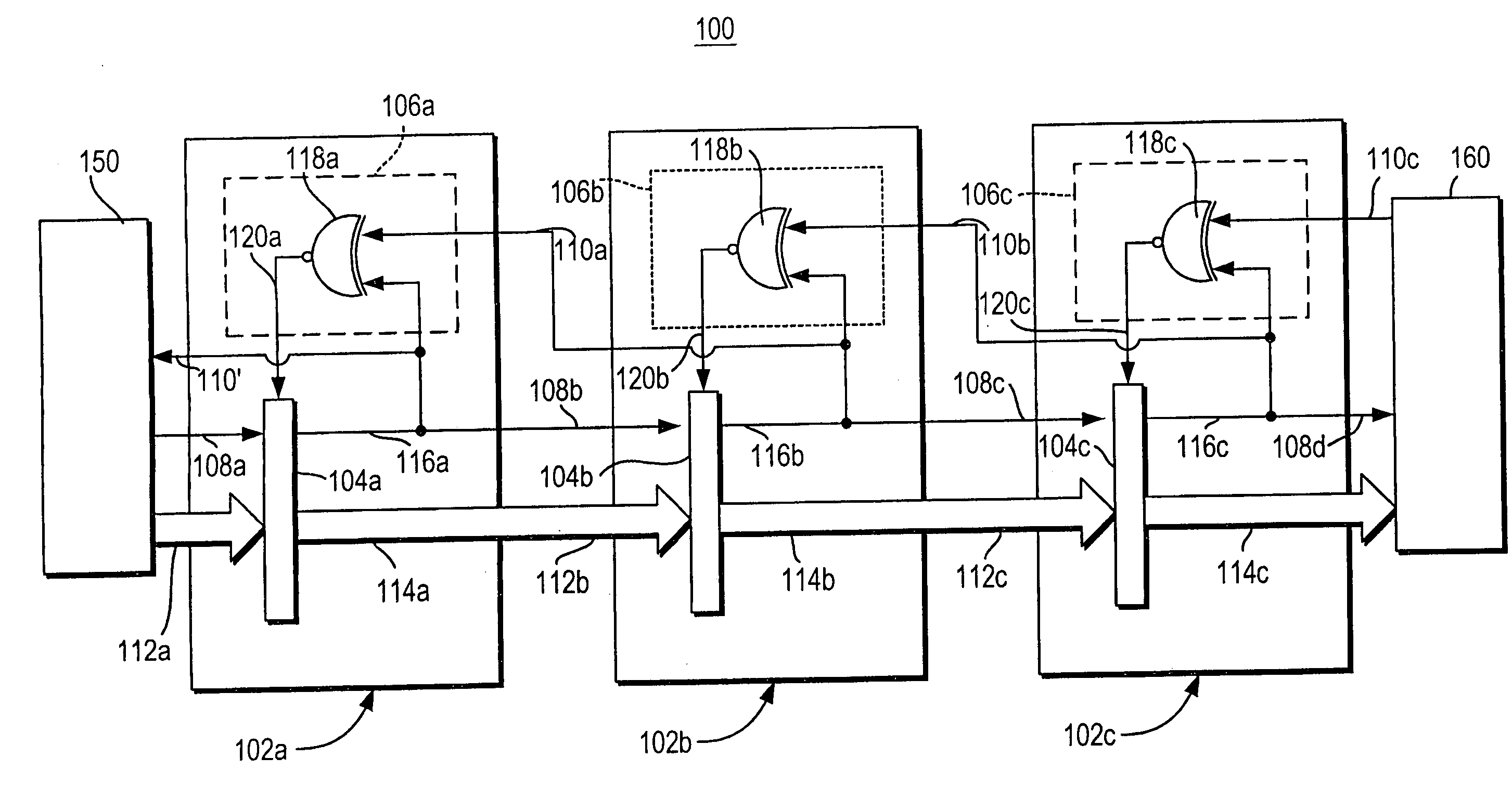
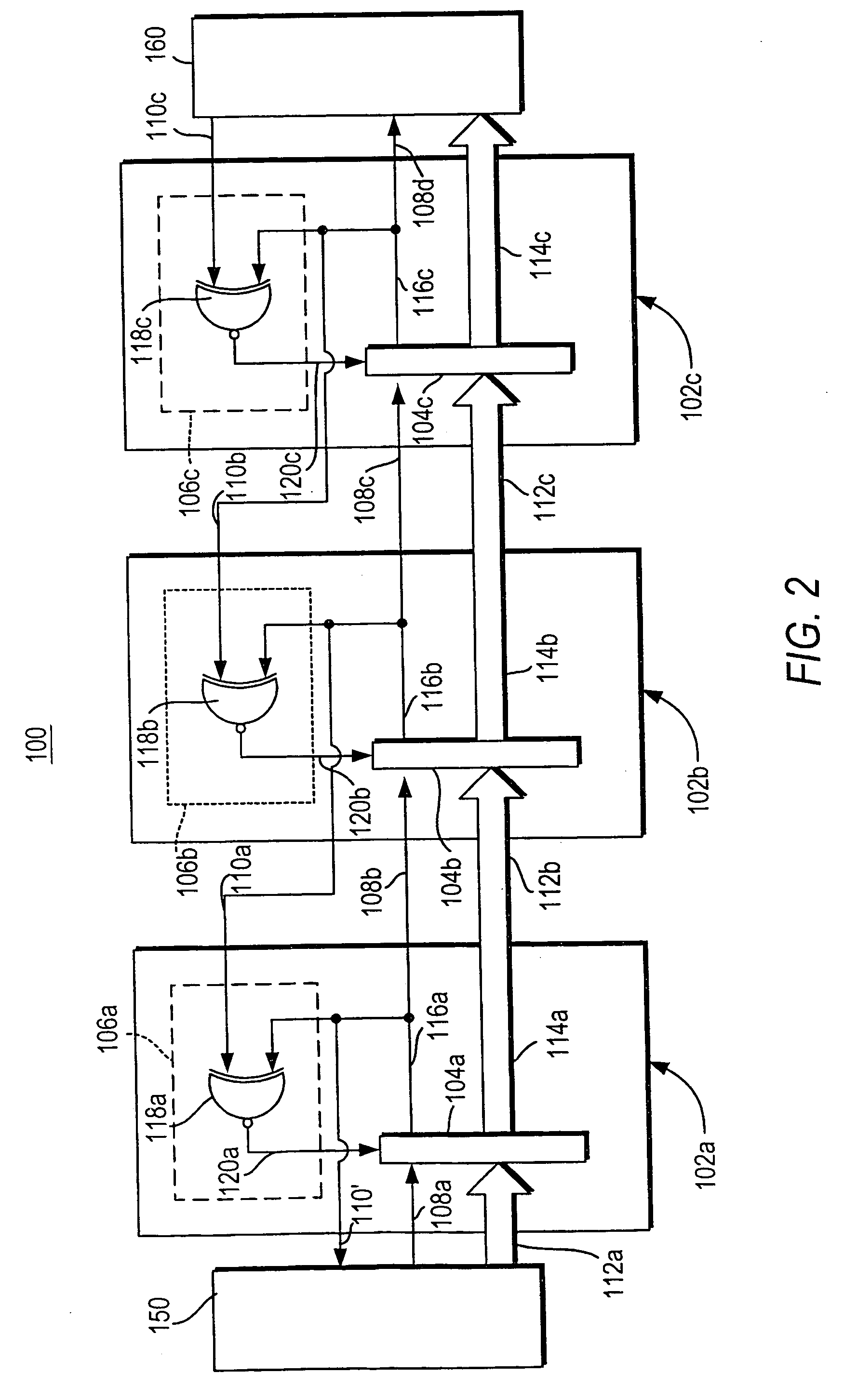
[0061] FIG. 4 illustrates the pipeline, referred to as pipeline 200, in which logic processing has been added. Pipeline 200 is substantially identical to pipeline 100, with the differences noted herein. As with pipeline 100, pipeline 200 has several stages, i.e., stage N-1 202a, stage N 202b, and stage N+1 202c. As with pipeline 100, each stage 202a, 202b, 202c comprises a data latch 204a, 204b, 204c and a latch controller 206a, 206b, 206c. The latch controller 206a, 206b, 206c comprises and XNOR element 218a, 218b, 218c. In pipeline 200, blocks of combinational logic 230a, 230b, 230c and matching delay elements 232a, 232b, 232c are inserted between adjacent pipeline stages. For example, if a stage implements a 32-bitwise OR function on two 32-bit operands, A.sub.0 . . . A.sub.31 and B.sub.0 . . . B.sub.31, then the logic would consist of 32 two-input OR gates computing A.sub.0+B.sub.0, A.sub.1+B.sub.1, etc. The datapath for a stage, e.g., stage N-1 202a, comprises the passage of da...
third embodiment
[0063] In accordance with a third embodiment, a goal of extremely high throughput may be achieved by "gate-level pipelines." In this embodiment, the datapath is sectioned into the finest-grained stages, each comprising a single level of logic with no explicit latches. As an additional benefit, the absence of latches provides savings of chip area and power consumption.
[0064] "Clocked-logic," also known as "clocked-CMOS" or "C.sup.2MOS," is a particularly attractive approach to gate-level pipelining. (Further details of clocked CMOS circuitry are described in M. Borah et al., "High-Throughput and Low-Power DSP Using Clocked-CMOS Circuitry, Proc. Intl. Symp. out Low-Power Design, 1995, pp.139-144, which is incorporated by reference in its entirety herein.) In the C.sup.2MOS scheme, separate, explicit latches are eliminated. Instead, a clock is applied directly to the logic gate. FIGS. 5-7 illustrate the structure of several exemplary C.sup.2MOS gates. For example, FIG. 5 illustrates a ...
example
[0101] Simulations were carried out for several of the pipeline styles described herein, using HSPICE, for a basic pipeline, such as pipeline 100, above. A simple 10-stage FIFO was simulated (with no logic processing) on a 16-bit wide datapath. The FIFO was designed and simulated in two different CMOS technologies: (i) a Taiwan Semiconductor Manufacturing Company (TSMC) 0.25 micron CMOS process, which is well-known in the art, and (ii) a 0.6 .mu.m Hewlett-Packard (HP) CMOS14TB process, which is also well-known in the art. For the first technology, only the unoptimized pipeline style was used: we did not include the "waveform shaping" optimization described above. For the second technology, both the optimized and the unoptimized versions of the pipeline were simulated. In each case, careful transistor sizing was used to improve performance.
[0102] The first simulation, using the 0.25 .mu.m TSMC process, was performed assuming a 2.5V power supply, 300K temperature, and a normal process...
PUM
 Abstract
Description
Claims
Application Information
 - R&D
- Intellectual Property
- Life Sciences
- Materials
- Tech Scout
- Unparalleled Data Quality
- Higher Quality Content
- 60% Fewer Hallucinations
Browse by: Latest US Patents, China's latest patents, Technical Efficacy Thesaurus, Application Domain, Technology Topic, Popular Technical Reports.
© 2025 PatSnap. All rights reserved.Legal|Privacy policy|Modern Slavery Act Transparency Statement|Sitemap|About US| Contact US: help@patsnap.com


