Water-soluble electrically conductive composition, modifications, and applications thereof
a technology of electrically conductive composition and water-soluble emulsion, which is applied in the direction of non-metal conductors, conductors, metal/alloy conductors, etc., can solve the problems of high cost and environmental hazards of many of these processes and materials, use expensive and toxic chemicals in product fabrication, and by-products of this process are typically expensive to recycle, so as to reduce the cost of process and process. cost, the effect of reducing the cost of process
- Summary
- Abstract
- Description
- Claims
- Application Information
AI Technical Summary
Benefits of technology
Problems solved by technology
Method used
Image
Examples
example
[0064] i. A first component stage containing substantially: (B) 82% of a thermoplastic acrylic-styrene copolymer emulsion,
[0065] ii. A second component stage containing substantially: (C) 10.7% of a wetting agent, such as ethylene glycol n-butyl ether; (K) 0.46% of a ductility agent such as dibutyl phthalate; and (E) 1.94% of deionized water,
[0066] iii. A third component stage containing substantially: (G) 0.34% of a surfactant, such as an acrylate copolymer with traces of 2-ethylhexyl acrylate and ethyl acrylate; and (E) 4.56% of deionized water.
[0067] The electrically insulative composition is comprised of component stages, similar to the electrically conductive inventive composition. The electrically insulative composition stages must be introduced in the order shown. All three stages must be premixed. Optimal mixing temperatures are between 15 and 25 degrees C. The optimum pH for the finished electrically insulative compostion is in a range of 6 to 8.
[0068] iii. Conductivity Mod...
embodiment 10
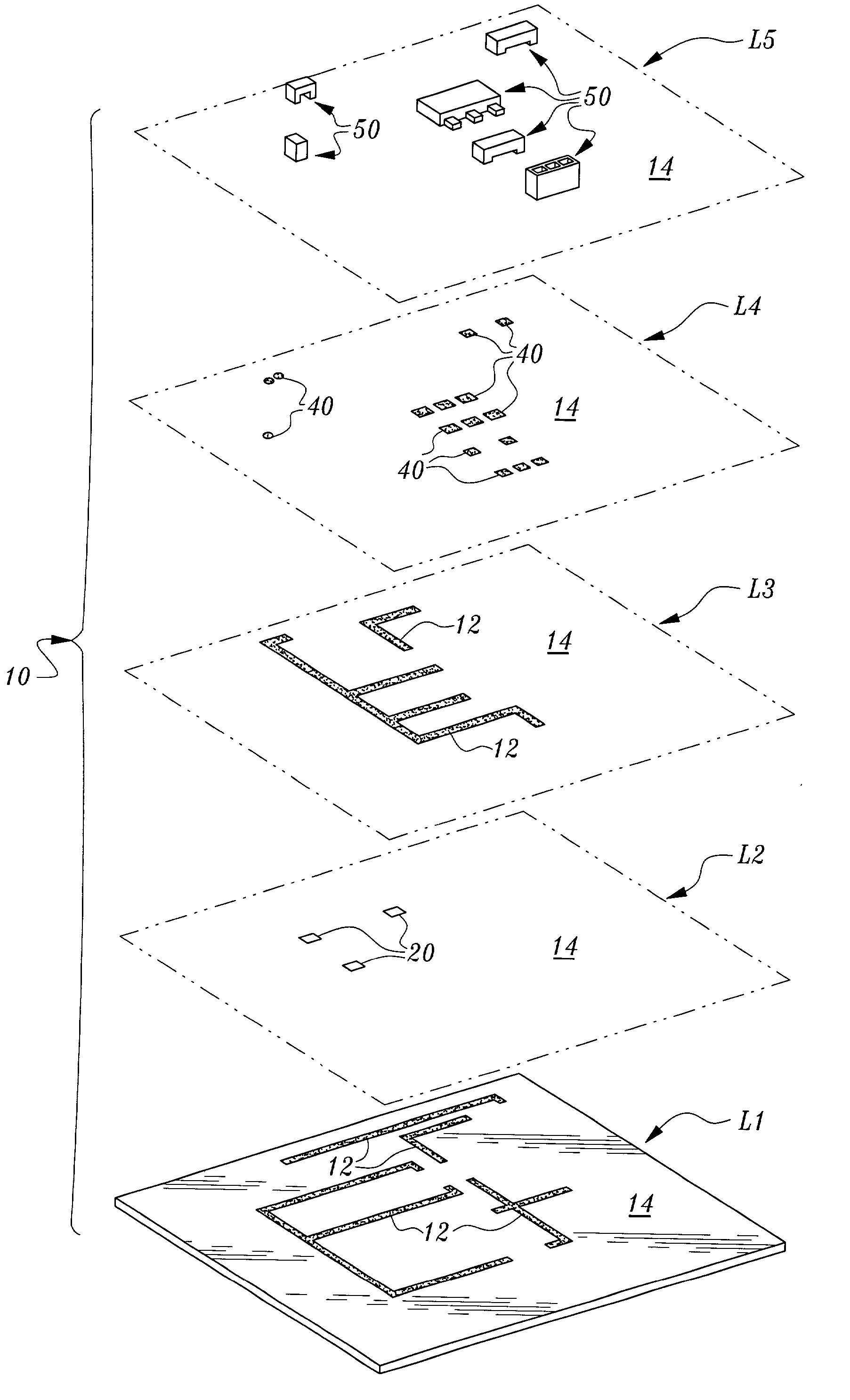
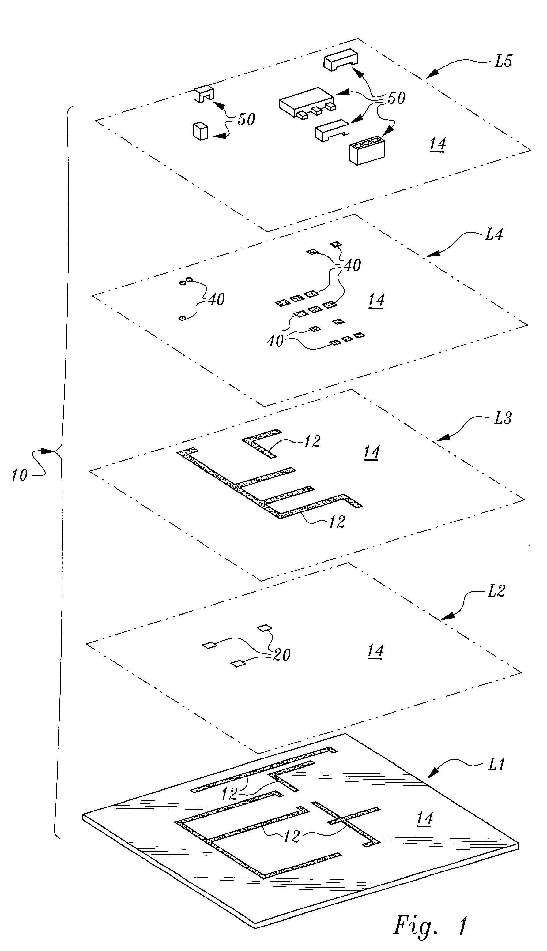
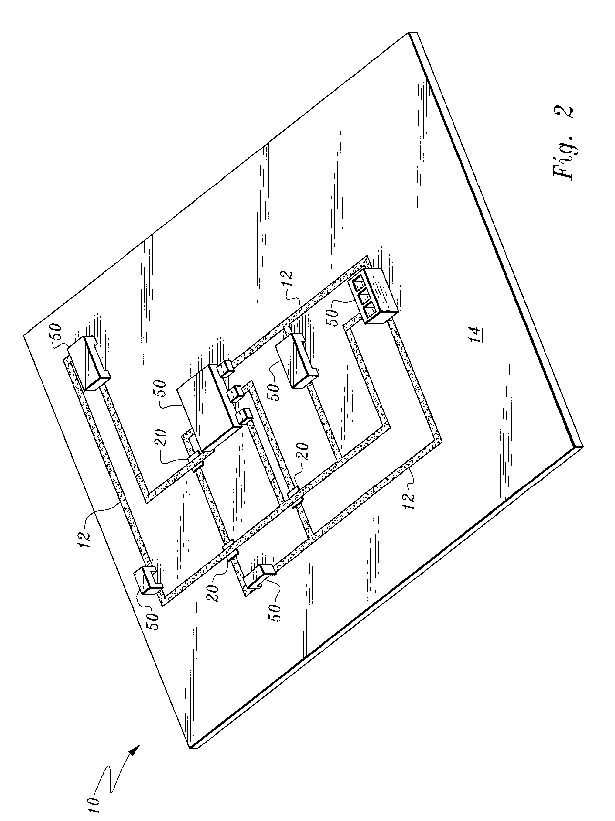
[0087] The first layer of the present invention, denoted "L1", is comprised of the first electrically conductive traces 12 applied to the substrate 14. Each of the remaining layers L2-L5 are likewise eventually applied to substrate 14 during manufacturing. In FIG. 1, layers L2-L5 are shown as imaginary planes with numbered components associated with each layer. Layers L2-L5, give the components positionings in space, relative to the components of other layers, and relative to the substrate 14 to which they will eventually be applied. FIG. 2 shows this eventual application of all the layers L1-L5 upon substrate 14 to form a printed circuit board 10. On L1, traces 12 are comprised of the electrically conductive polymer. The present invention is compatible with numerous substrates: three-dimensional, extremely smooth, extremely rough, porous, distressed, electrically conductive or flexible, etc. However, in the case of fabricating circuit boards using the inventive electrically conduct...
PUM
| Property | Measurement | Unit |
|---|---|---|
| diameter | aaaaa | aaaaa |
| specific gravity | aaaaa | aaaaa |
| widths | aaaaa | aaaaa |
Abstract
Description
Claims
Application Information
 - R&D
- Intellectual Property
- Life Sciences
- Materials
- Tech Scout
- Unparalleled Data Quality
- Higher Quality Content
- 60% Fewer Hallucinations
Browse by: Latest US Patents, China's latest patents, Technical Efficacy Thesaurus, Application Domain, Technology Topic, Popular Technical Reports.
© 2025 PatSnap. All rights reserved.Legal|Privacy policy|Modern Slavery Act Transparency Statement|Sitemap|About US| Contact US: help@patsnap.com


