
Generation and use of integrated circuit profile-based simulation information

a technology of integrated circuits and simulation information, which is applied in the field of integrated circuit (ic) manufacture, can solve the problems of insufficient information available early and/or in line with the fabrication process, cost-rework or unusable end products, and batch affected wafers may have to be discarded

Active Publication Date: 2003-08-28
TOKYO ELECTRON US HOLDINGS INC
View PDF12 Cites 55 Cited by
  • Summary
  • Abstract
  • Description
  • Claims
  • Application Information

AI Technical Summary

Benefits of technology

0036] Still referring to FIG. 5A, the profile data of the best matching profile library instance are transmitted to the device simulator 113. Profile data comprises critical dimensions, profile shape description, and profile graphic representation. Critical dimensions are typically expressed as measurement dimensions, for example, width of 50 nanometers. Alternatively, critical dimensions are also expressed as a percent of another critical dimension, for example, 80% height of top rounding meaning the structure top starts rounding at 80% of the structure's height. An example of profile shape description is trapezoidal with top rounding profile. An example of profile graphic representation is a bit map of the profile. The device simulator 113 may be any type of device simulator simulating electrical, thermal, noise, 3D effects, steady or transient state signal, leakage and/or optical characteristics. Examples of device simulators are Raphael.TM, Medici.TM, ATLAS.TM, and TMA-Visual.TM from companies such as Avant!, Technology Modeling Associates, and Silvaco International. The profile critical dimensions of the best matching library instance from the calculated signals library is extracted by the profiler application server 109 and transmitted to the device simulator 113. The device simulator 113 creates as output the set of process control parameters used in the simulation run and the resulting device attributes. For example, if the device simulator is an interconnect simulator, the input may be the top and bottom CD's in nanometers, and the sidewall angle in degrees in a format required by the interconnect simulator used. The output of the device simulator 113 is device attributes including resistance in ohms, capacitance in farads, and inductance in henrys. The simulation data store generator 111 creates a data store instance comprising signals, profile data, simulation type, and device attributes associated with the specific device simulation. Simulation type is the characterization of the simulation being performed, for example device simulation. A partial list of simulation types is included in FIG. 10.
0037]...

Problems solved by technology

In many traditional IC manufacturing environments, the effect of a design decision or a fabrication process change is frequently not immediately known by the designers or the process engineers until much later, resulting in costly rework or unusable end products.
However, if a design did not produce the desired results or a process change caused some key critical dimension (CD) of the structures to be out of the acceptable ranges, the batch of wafers affected may have to be discarded.
Even with the use of current design and fabrication process simulators, there is typically insufficient information available early and / or in-line with the fabrication process.
Other simulators attempt to model complex shapes with limited success due to the number of variables during fabrication.

Method used


Image

  • Generation and use of integrated circuit profile-based simulation information
  • Generation and use of integrated circuit profile-based simulation information
  • Generation and use of integrated circuit profile-based simulation information

Examples


Embodiment Construction

)

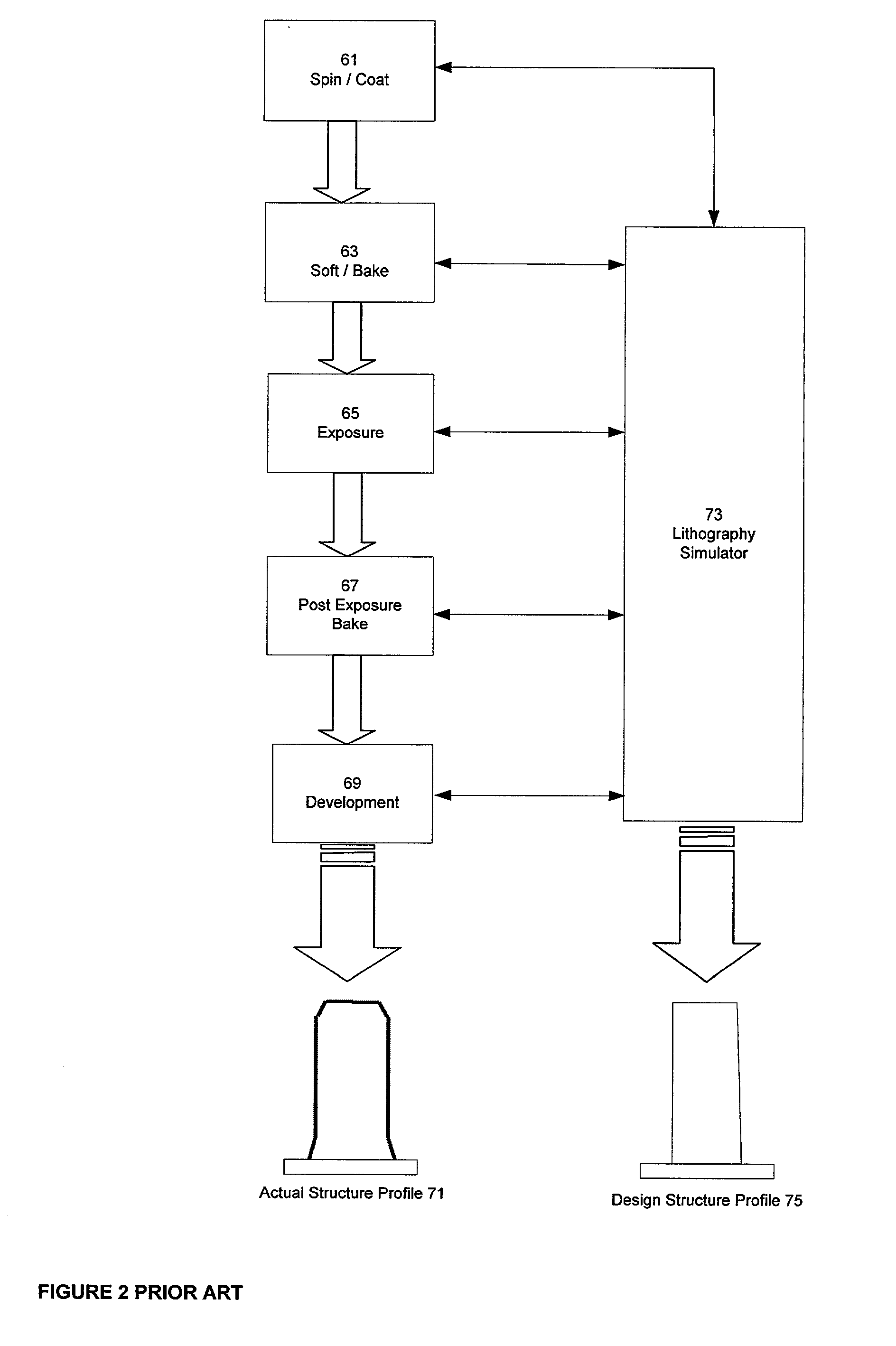
[0030] The invention includes a method and a system for creating and using a data store of profile-based simulation information. FIGS. 2 and 3 illustrate the differences between simulation profiles versus actual profiles of structures. FIGS. 4 to 8C depict embodiments of the creation process for the profile-based simulation data store. FIGS. 9A and 9B depict embodiments for using the profile-based simulation information. FIG. 10 illustrates one format of the simulation data store, while FIGS. 11A and 11B represents empirical data that illustrate the utility of the concepts and principles of the present invention.

[0031] FIG. 2 is a prior art architectural diagram contrasting the layer feature profile of actual lithography process steps versus the feature profile generated in a typical lithography simulator. A lithography simulator 73 simulates the actual physical processes including spin / coat 61, soft bake 63, exposure 65, post exposure bake 67, and development 69 processes. The act...


PUM


Abstract

The invention includes a method and a system for generating integrated circuit (IC) simulation information regarding the effect of design and fabrication process decisions. One embodiment includes creating and using a data store of profile-based information comprising metrology signal, structure profile data, process control parameters, and IC simulation attributes. Another embodiment is a method and system for generating a simulation data store using signals off test gratings that model the effect of an IC design and / or fabrication process. One application includes creation and use of a simulation data store generated using test gratings that model the geometries of the IC interconnects. The interconnect simulation data store may be used in-line for monitoring electrical and thermal properties of an IC device during fabrication. Other embodiments include methods and systems for generating and using simulation data stores utilizing a metrology simulator and various combinations of a fabrication process simulator, a device simulator, and / or circuit simulator. Information from the simulation data store may be used in-line in-situ during the design or fabrication process steps.

Description

[0001] This application relates to co-pending U.S. patent application Ser. No. 09 / 727,530 entitled "System and Method for Real-Time Library Generation of Grating Profiles" by Jakatdar, et al., filed on Nov. 28, 2000, owned by the assignee of this application and incorporated herein by reference and to co-pending U.S. patent application Ser. No. 09 / 764,780 entitled "Caching of Intra-Layer Calculations for Rapid Rigorous Coupled-Wave Analyses" by Jakatdar, et al., filed on Jan. 26, 2000, owned by the assignee of this application and incorporated herein by reference.BACKGROUND OF INVENTION[0002] 1. Field of Invention[0003] The present application relates to the general area of integrated circuit (IC) manufacture and more particularly to methods and systems for creating and using a data store of profile-based simulations information.[0004] 2. Related Art[0005] With the demand for increasing clock rates and decreasing geometries of IC structures, there is a need for rapid feedback on the...

Claims


Application Information

Patent Timeline
IPC IPC(8): G06F17/50G06F19/00H01L21/00H01L21/66
CPCG06F2217/80G06F17/5009G06F2119/08G06F30/20
Inventor JAKATDAR, NICKHILNIU, XINHUIBAO, JUNWEI
Owner TOKYO ELECTRON US HOLDINGS INC
Learn More