
Semiconductor wafer and vapor phase growth apparatus

a technology of vapor phase and semiconductor wafer, which is applied in the direction of crystal growth process, polycrystalline material growth, transportation and packaging, etc., can solve the problems of complex adjustment of dopant gas flow rate, non-realistic, and problematic leakage of current in circui

Inactive Publication Date: 2003-03-06
SHIN-ETSU HANDOTAI CO LTD
View PDF13 Cites 12 Cited by
  • Summary
  • Abstract
  • Description
  • Claims
  • Application Information

AI Technical Summary

Benefits of technology

The solution enables the formation of semiconductor thin films with uniform resistivity distribution and minimal slip dislocations on large diameter substrates, enhancing semiconductor chip fabrication throughput and yield by allowing precise resistivity control and maintaining uniformity across the substrate.

Problems solved by technology

If an integrated circuit is fabricated in a region with slip dislocation generated, leakage of a current in the circuit occurs problematically.
With such regulation of heating powers, however, a resistivity of the peripheral portion of the silicon single crystal thin film 32 is deviated from that of the central portion thereof, a problem again arises, since a resistivity distribution along a diameter of the silicon single crystal thin film 32 becomes non-uniform.
However, according to this method, since a dopant flow rate is necessary to be adjusted at each inlet port 18a to 18f, a problem has arisen since actual adjustment of the dopant gas flow rates is very complex and non-realistic.

Method used


Image

  • Semiconductor wafer and vapor phase growth apparatus
  • Semiconductor wafer and vapor phase growth apparatus
  • Semiconductor wafer and vapor phase growth apparatus

Examples


example

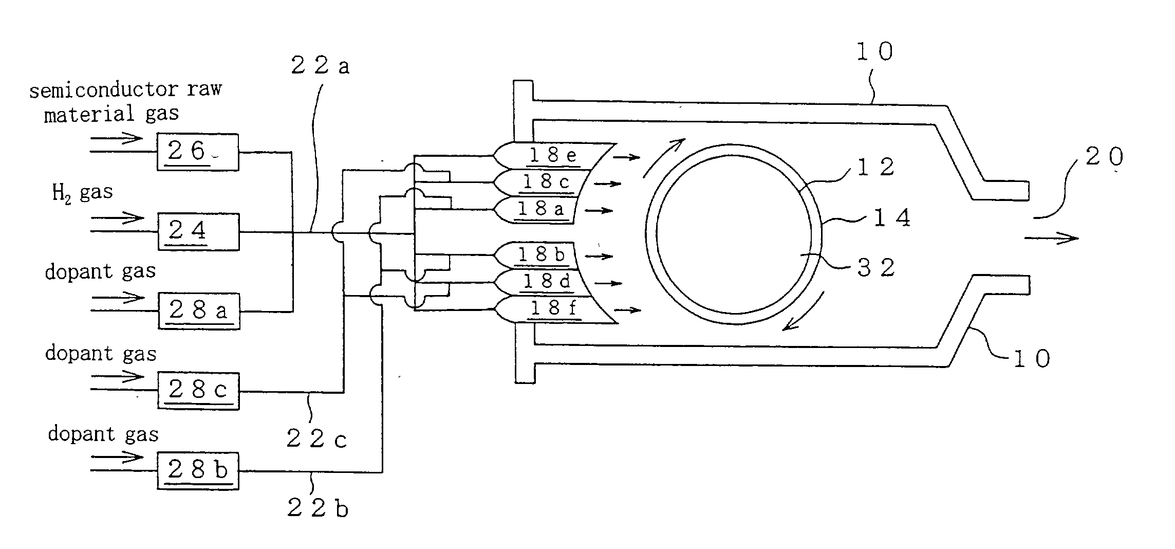
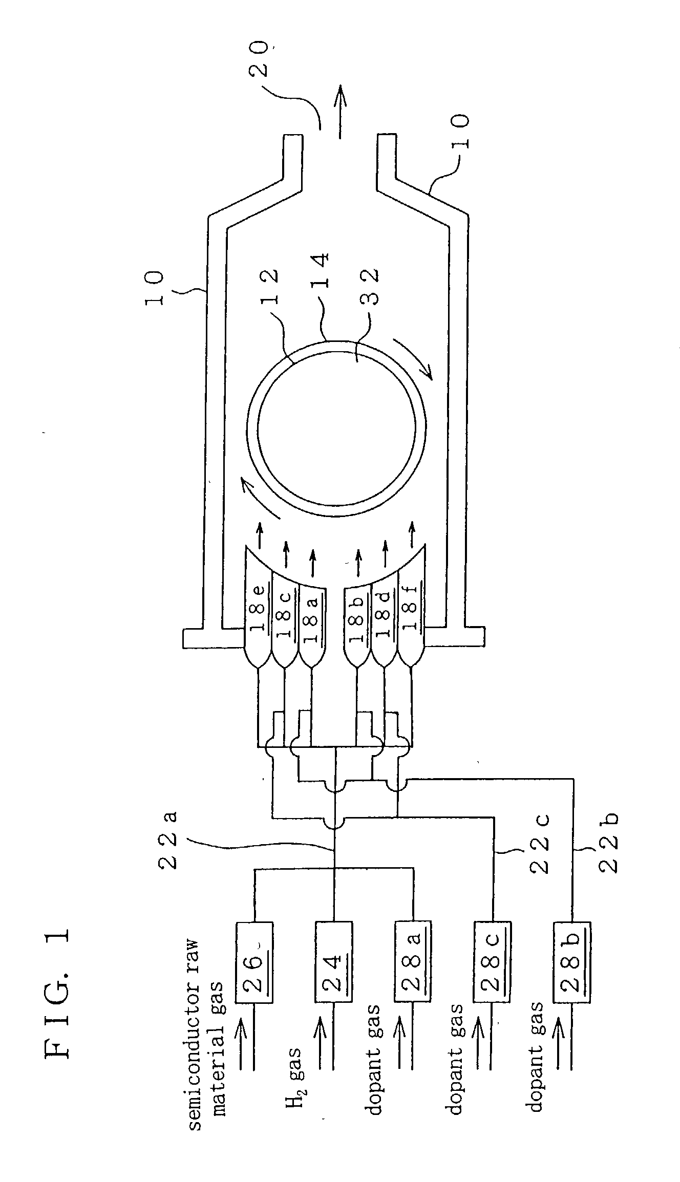
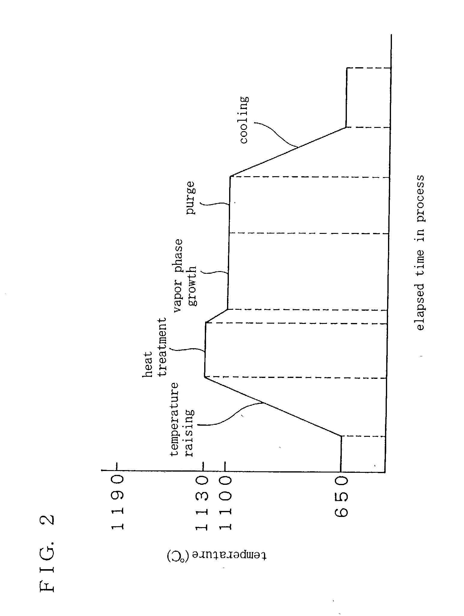
[0065] Description will be made, using FIGS. 2 and 3, of concrete operating conditions for formation of a silicon single crystal thin film on a main surface of silicon single crystal substrate using the horizontal, single wafer vapor phase growth apparatus shown in FIGS. 1 and 6, and a resistivity distribution of a silicon single crystal thin film 32 thus formed under the concrete operating conditions.

[0066] FIG. 2 is a graph showing a temperature programme in production of a semiconductor wafer using the vapor phase growth apparatus shown in FIG. 1 and FIG. 3 is a graph showing a resistivity distribution along a diameter of a semiconductor wafer produced using the vapor phase growth apparatus of FIG. 1.

[0067] As the silicon single crystal substrate 12 placed on the susceptor 14 in the reaction chamber 10, there is used a p-type silicon single crystal substrate 12 of 300 mm .+-.0.2 mm in diameter and of a resistivity in the range of from 1.OMEGA..multidot.cm to 20.OMEGA..multidot.cm...


PUM

PropertyMeasurementUnit
resistivityaaaaaaaaaa

Abstract

It is an object of the present invention to provide not only a semiconductor wafer obtained by forming a semiconductor thin film with uniform resistivity and substantially no slip dislocation on a main surface of a semiconductor single crystal substrate having a relatively low dopant concentration, as large as 300 mm or more in diameter but also a vapor phase growth apparatus by means of which such a semiconductor wafer can be produced. A dopant gas is supplied into a reaction chamber 10 through all of the inlet ports 18a to 18f disposed in a width direction of the reaction chamber 10 from a common gas pipe 22a functioning as a main dopant gas pipe. Further, the dopant gas is additionally supplied through inner inlet ports 18a and 18b, and middle inlet ports 18c and 18d, as specific gas inlet ports, into the reaction chamber 10 from first and second auxiliary dopant gas pipes 22b and 22c.

Description

[0001] This invention relates to a semiconductor wafer and a vapor phase growth apparatus and particularly, a semiconductor wafer obtained by forming a semiconductor thin film having a uniform resistivity distribution on a main surface of a large diameter semiconductor single crystal substrate and a vapor phase growth apparatus employed for producing the semiconductor wafer.[0002] In company with recent miniaturization of an electronic device, not only has the use of semiconductor wafers each obtained by forming a silicon single crystal thin film on a main surface of a silicon single crystal substrate increased, but a more uniform resistivity distribution of the silicon single crystal thin film has also been required. The term "uniform resistivity distribution" used here, to be detailed, means that a resistivity distribution across the surface of the silicon single crystal thin film is uniform. Further, a larger diameter has also been demanded on a semiconductor wafer together with ...

Claims


Application Information

Patent Timeline
Patent Type & Authority Applications(United States)
IPC IPC(8): C23C16/44C23C16/455C30B25/02C30B25/14H01L21/205
CPCC23C16/45561C23C16/45563C23C16/45574C30B25/14C30B29/06Y10T428/12528H01L21/02532H01L21/02579H01L21/0262Y10T428/31Y10T428/21H01L21/02381
Inventor OSE, HIROKI
Owner SHIN-ETSU HANDOTAI CO LTD
Learn More