
High-frequency circuit board unit, high frequency module using the same unit, electronic apparatus using the same module, and manufacturing method for the high-frequency circuit board unit

a manufacturing method and technology for high-frequency circuit boards, applied in the direction of electrical apparatus, semiconductor devices, semiconductor/solid-state device details, etc., can solve the problems of increasing the cost of carrying out process steps, damage to semiconductor devices, and damage to semiconductor devices

Inactive Publication Date: 2002-06-13
MURATA MFG CO LTD
View PDF1 Cites 80 Cited by
  • Summary
  • Abstract
  • Description
  • Claims
  • Application Information

AI Technical Summary

Benefits of technology

[0024] The high-frequency circuit board unit, the high-frequency module, and the electronic apparatus of the present invention provide a high breakdown voltage against an electrostatic surge voltage. Thus, the reliability can be improved, and the size of the high-frequency circuit board unit can be reduced.
[0025] According to the manufacturing method for the high-frequency circuit board of the present invention, the possibility of electrostatic discharge damage while manufacturing the semiconductor device can be reduced. As a result, the manufacturing process can be simplified, and the cost of the high-frequency circuit board unit can be reduced.

Problems solved by technology

Generally, however, the semiconductor device 8, in particular, a GaAs semiconductor device, has a low breakdown voltage, and an electrostatic surge voltage may cause electrostatic discharge damage to the semiconductor device 8.
Thus, if a surge voltage is applied to the circuit board unit via this terminal electrode, the semiconductor device may be damaged.
However, this increases the cost of carrying out the process steps.
With this measure, however, the semiconductor device becomes expensive, and the diode may cause the loss of a high-frequency signal.

Method used


Image

  • High-frequency circuit board unit, high frequency module using the same unit, electronic apparatus using the same module, and manufacturing method for the high-frequency circuit board unit
  • High-frequency circuit board unit, high frequency module using the same unit, electronic apparatus using the same module, and manufacturing method for the high-frequency circuit board unit
  • High-frequency circuit board unit, high frequency module using the same unit, electronic apparatus using the same module, and manufacturing method for the high-frequency circuit board unit

Examples


Embodiment Construction

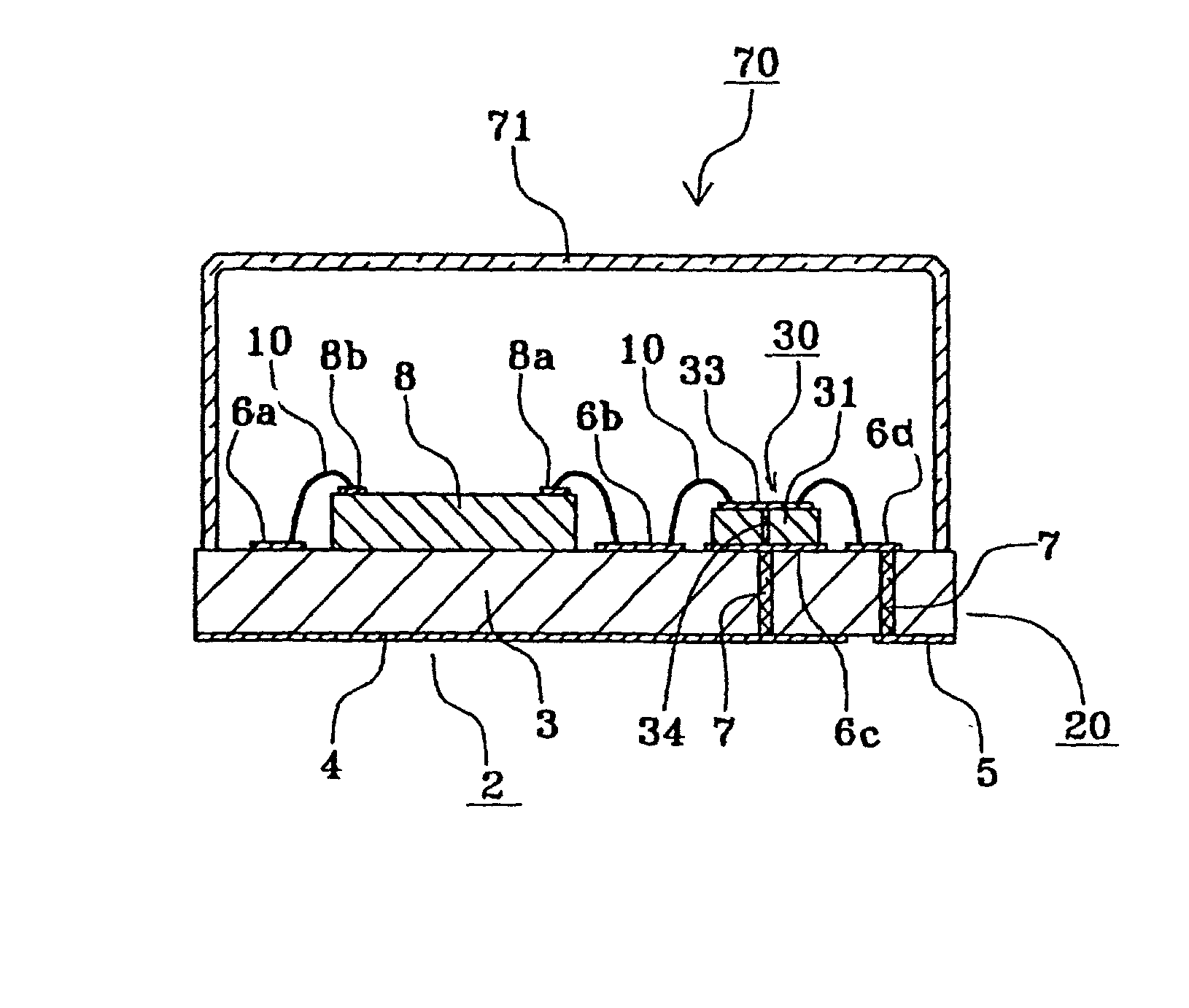
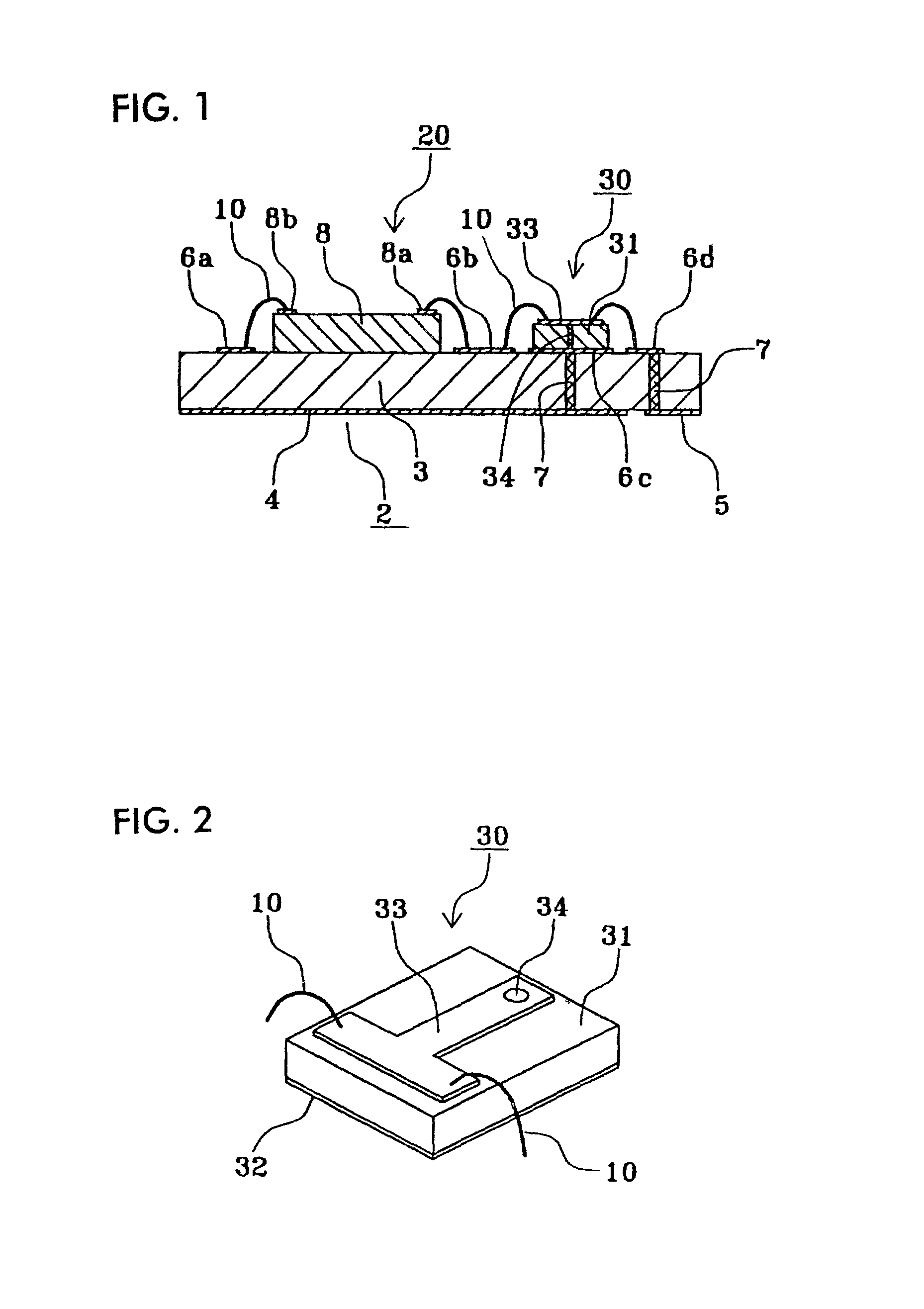
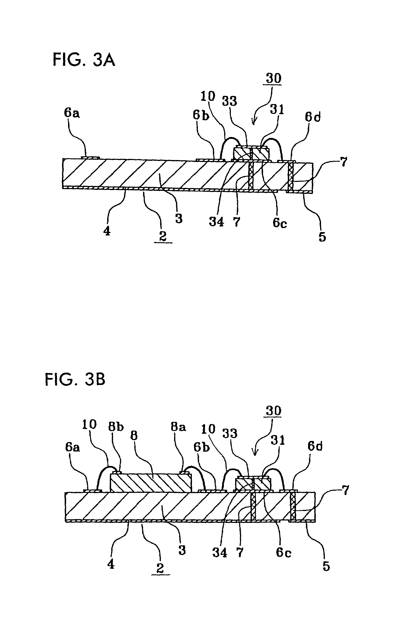
[0039] FIG. 1 is a sectional view illustrating a high-frequency circuit board unit according to an embodiment of the present invention. In FIG. 1, elements the same as or similar to those of FIG. 11 are designated with like reference numerals, and an explanation thereof will thus be omitted.

[0040] In a high-frequency circuit board unit 20 shown in FIG. 1, the semiconductor device 8 and a filter 30, which serves as a passive impedance circuit device, are connected to a plurality of wiring electrodes 6a, 6b, 6c, 6d which are formed on the second main surface of the dielectric substrate 3. Unlike the conventional high-frequency circuit board unit 1 shown in FIG. 11, the wiring electrode 6a connected to the connecting land 8b via the wire 10 is not connected to a terminal electrode on the first main surface of the dielectric substrate 3.

[0041] FIG. 2 is a perspective view illustrating the filter 30. In FIG. 2, the filter 30 includes a dielectric substrate 31, a ground electrode 32, a st...


PUM


Abstract

A ground electrode and a terminal electrode are formed on a first main surface of dielectric substrate forming a circuit board. Wiring electrodes are formed on a second main surface of the dielectric substrate. A semiconductor device and a filter are mounted on the wiring electrodes. A strip line electrode of the filter is connected to the ground electrode of the circuit board for conducting direct current, via a through-hole provided in the filter, a ground electrode of the filter, the wiring electrode, and a through-hole provided in the circuit board. With this arrangement, the terminal electrode is connected to a high-frequency signal terminal of the semiconductor device via the filter.

Description

[0001] 1. Field of the Invention[0002] The present invention relates to a high-frequency circuit board unit, a high-frequency module using the same unit, and an electronic apparatus using the same module. The invention also relates to a manufacturing method for the above-described high-frequency circuit board unit.[0003] 2. Description of the Related Art[0004] FIG. 11 is a sectional view illustrating a conventional high-frequency circuit board unit. In FIG. 11, a high-frequency circuit board unit 1 includes a circuit board 2, a semiconductor device 8, and a filter 15 which serves as a passive impedance circuit device. The circuit board 2 has a dielectric substrate 3, which is formed of a dielectric material, such as an alumina substrate, having a comparatively low dielectric constant (of about 9 to 10). A ground electrode 4 and terminal electrodes 5a, 5b are formed on a first main surface of the dielectric substrate 3. Wiring electrodes 6a, 6b, 6c, 6d are formed on a second main sur...

Claims


Application Information

Patent Timeline
Patent Type & Authority Applications(United States)
IPC IPC(8): H01L23/12H01L23/00H01L23/66H01L25/00
CPCH01L23/66H01L2924/19105H01L2224/16225H01L2224/48091H01L2224/48227H01L2924/01004H01L2924/01013H01L2924/01033H01L2924/01051H01L2924/01078H01L2924/15313H01L2924/16152H01L2924/30107H01L2924/3011H01L24/73H01L2924/12041H01L24/48H01L2924/01005H01L2924/01072H01L2924/10329H01L2224/32225H01L2224/73265H01L2924/15192H01L2924/00014H01L2924/00012H01L2924/00H01L2224/05599H01L2224/45099H01L2224/85399H01L2224/45015H01L2924/207
Inventor SAYANAGI, KAZUYASASABATA, AKIHIROSASAKI, YUTAKA
Owner MURATA MFG CO LTD
Learn More