
Metal contact structure in semiconductor device and method for forming the same

Inactive Publication Date: 2002-06-13
SAMSUNG ELECTRONICS CO LTD
View PDF0 Cites 192 Cited by
  • Summary
  • Abstract
  • Description
  • Claims
  • Application Information

AI Technical Summary

Problems solved by technology

As the integration density of a semiconductor device increases and thus, the width of the conductive layer (the wiring) is reduced and the aspect ratio of the contact hole increases, many problems occur in forming the metal contact structure.
Also, contact resistance increases and contact reliability deteriorates due to a void or a key hole generated when a metal is deposited in a high aspect ratio contact hole.
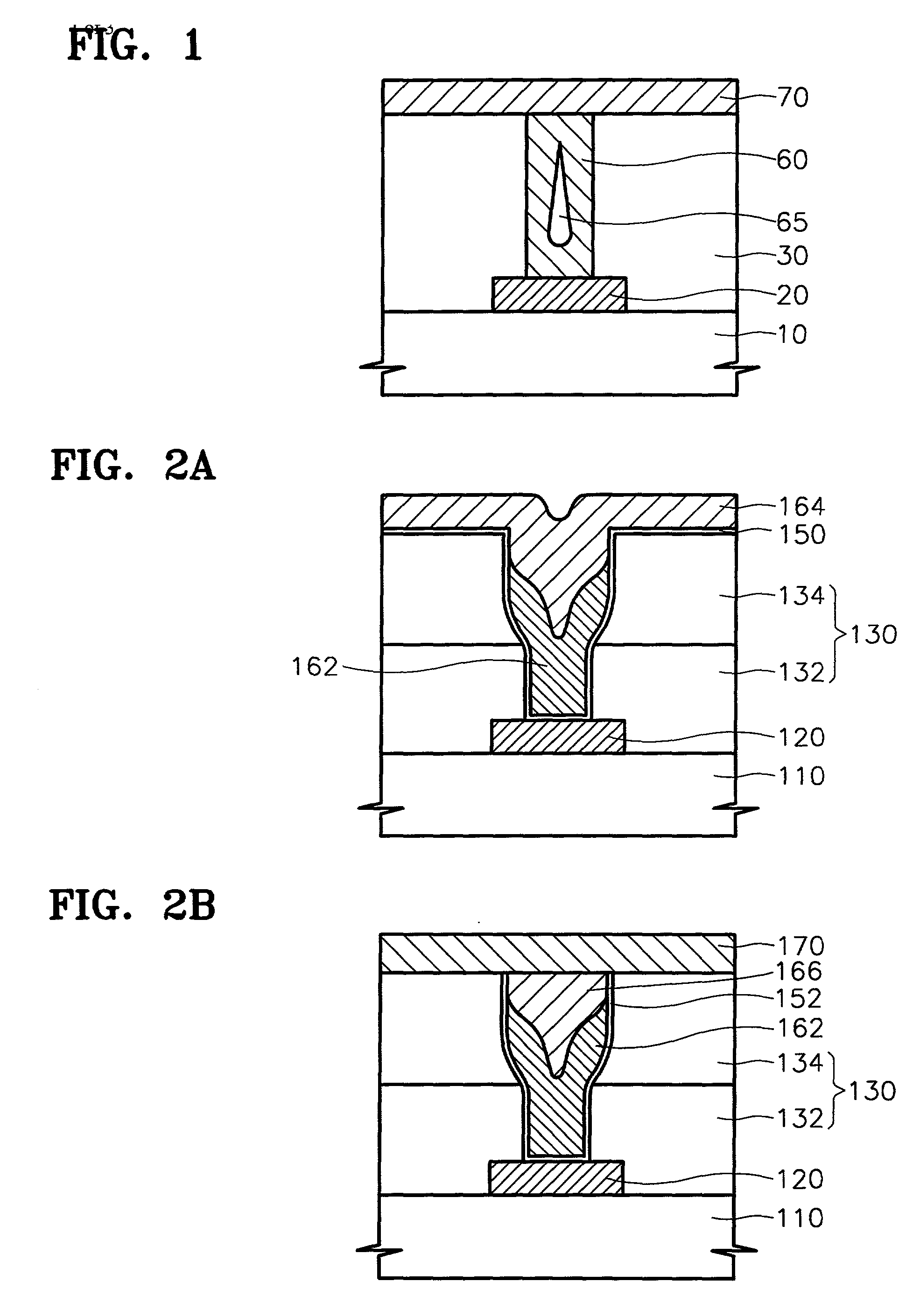
The void 65 or the key hole increases the contact resistance and deteriorates the reliability of the contact.
However, in such a method, problems may occur since tungsten is unevenly removed when the etching uniformity of the entire wafer during the etch back of tungsten is considered.
However, the method is susceptible to the generation of a void and is not productive since a photolithography process and an ion implantation process must be performed.

Method used


Image

  • Metal contact structure in semiconductor device and method for forming the same
  • Metal contact structure in semiconductor device and method for forming the same
  • Metal contact structure in semiconductor device and method for forming the same

Examples


first embodiment

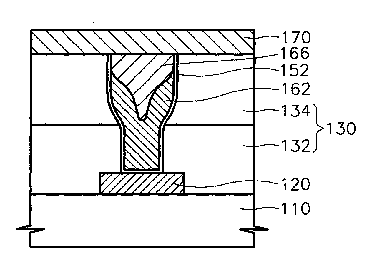
[0026] FIGS. 2A and 2B are sectional views showing a metal contact structure according to the present invention.

[0027] Referring to FIG. 2A, a predetermined lower conductive layer 120 is formed on a substrate 110. An interlayer dielectric film 130 overlies the substrate 110 including the lower conductive layer 120. A contact hole that exposes a region of the lower conductive layer 120 is formed in the interlayer dielectric film 130. An upper wiring comprises lower and upper metals layers 162 and 164 that fill the contact hole is formed. Reference numeral 150 denotes a barrier metal layer for preventing the metal that forms the upper wiring from being diffused to the lower conductive layer 120 and through the interlayer dielectric film 130. The barrier metal layer 150 is commonly formed by stacking a Ti film and a TiN film. However, the barrier metal layer 150 can be formed of other metal films such as a Ta film, a TaN film or a metal nitride film.

[0028] The lower conductive layer 12...

second embodiment

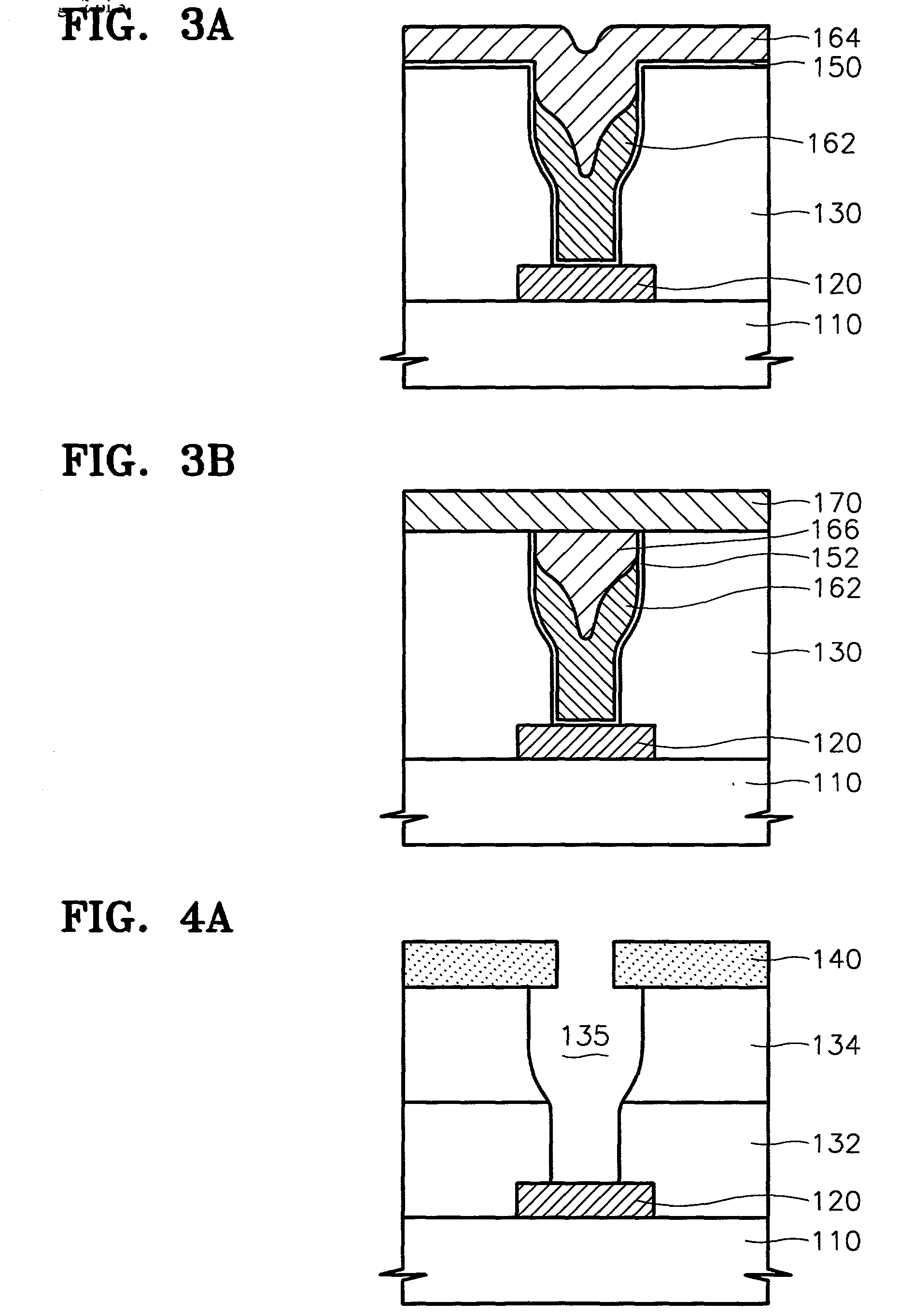
[0042] FIG. 5 is a sectional view showing the processes of forming the metal contact structure of a second embodiment as shown in FIGS. 3A and 3B. The metal contact structure shown in FIGS. 3A and 3B is different from the metal contact structure shown in FIGS. 2A and 2B only in that the interlayer dielectric film 130 is formed of a single layer as mentioned previously. Therefore, when the interlayer dielectric film 130 is formed of a single layer, only the processes of forming the contact hole having the same shape as shown in the above-mentioned embodiment are described and description of the remaining processes will be omitted.

[0043] As shown in FIG. 5, the lower conductive layer 120 and the interlayer dielectric film 130 are formed on the substrate 110 and then, the photoresist pattern 140 to define the contact hole 135 is formed. The upper portion of the contact hole 135 is previously formed by an isotropic etch using the photoresist pattern 140 as the etching mask. Then, the in...


PUM


Abstract

A metal contact structure of a semiconductor device and a method for forming the same are provided. The diameter of the upper portion of a contact hole that exposes a region of a lower conductive layer is formed to be larger than the diameter of the lower portion of the contact hole. The metal contact structure is formed without a void or a key hole. This is accomplished by forming at least two metal layers to fill the contact hole by performing a first deposition, an etch back, and a second deposition. The metal layer which fills the contact hole is etched back using a barrier metal layer formed on the entire surface of the contact hole as an etching stop layer. Thus, a void or key hole is not generated by making the upper portion of the contact hole to be wider than the lower portion of the contact hole and by depositing the metal which fills the contact hole through the processes of firstly depositing the metal, etching back the metal, and secondly depositing the metal.

Description

[0001] 1. Field of the Invention[0002] The present invention relates to a semiconductor device, and more particularly, to a metal contact structure in a semiconductor device and a method forming the same.[0003] 2. Description of the Related Art[0004] In general, a semiconductor device is formed by stacking a predetermined conductive layer and an interlayer dielectric film on a semiconductor substrate. The conductive layer includes a wiring through which an electrical signal is transmitted. Polycrystalline silicon doped with impurities is mainly used as a material for the wiring.[0005] Recently, attention has been devoted to a method of using a metal such as tungsten, aluminum, copper, or metal silicide, which has an excellent conductive characteristic, as the wiring material instead of polycrystalline silicon doped with impurities.[0006] In general, a metal wiring structure includes a wiring longitudinally extended in a horizontal direction parallel to the surface of a substrate and...

Claims


Application Information

Patent Timeline
IPC IPC(8): H01L21/28H01L21/768H01L23/522
CPCH01L21/76804H01L23/5226H01L21/76877H01L2924/0002H01L2924/00H01L21/28
Inventor SUN, HO-WONLEE, KANG-YOONKIM, JEONG-SEOKSHIN, DONG-WONCHO, TAI-HEUI
Owner SAMSUNG ELECTRONICS CO LTD
Learn More