Structured screens for controlled spreading of light
a structured screen and light technology, applied in the field of optical devices, can solve the problems of limited shaping over the resulting scattering, inability to achieve such accuracy, and inability to control the spreading pattern only to a limited degree, so as to achieve the effect of increasing numerical aperture and increasing peak intensity
- Summary
- Abstract
- Description
- Claims
- Application Information
AI Technical Summary
Benefits of technology
Problems solved by technology
Method used
Image
Examples
example 1
Effect of Microstructure Shape
[0182] This example illustrates the importance of the shape of each microstructure in tailoring the light spreading pattern.
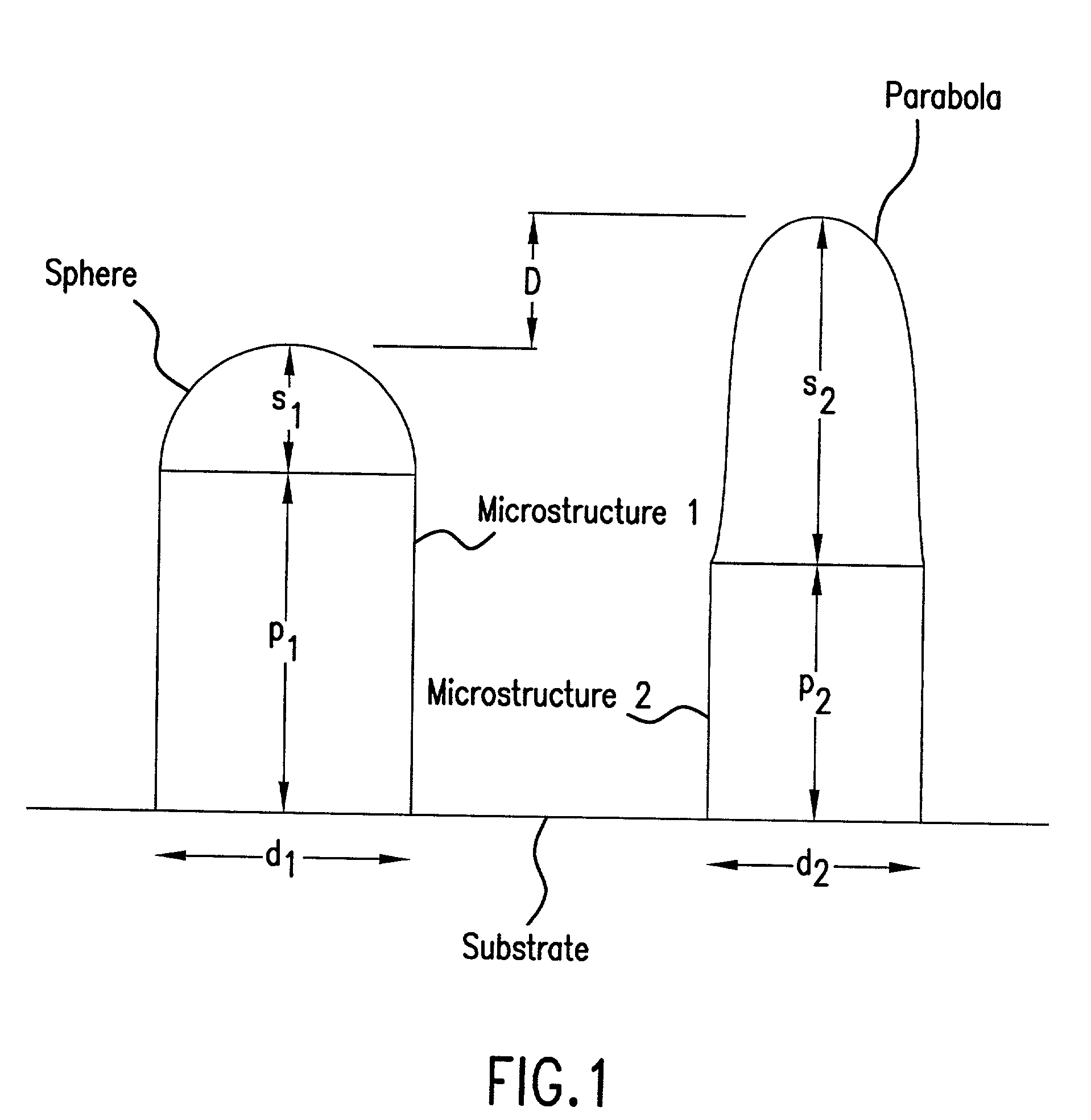
[0183] Initially we consider a regular array of identical microstructures with a shape that can be expressed as function of one or more parameters, some of which are random variables. For instance, a microstructure of spherical shape has a sag function that is given by R-(R.sup.2-r.sup.2).sup.1 / 2, where R denotes the radius of curvature and r denotes the radial position from the origin. According to this definition, the array consists of spherical microlenses with possibly variable radii of curvature. The size of each microstructure is identical throughout the screen surface, so that the presence of randomness is confined to a particular parameter, namely, the radii of curvature of the spherical microlenses.
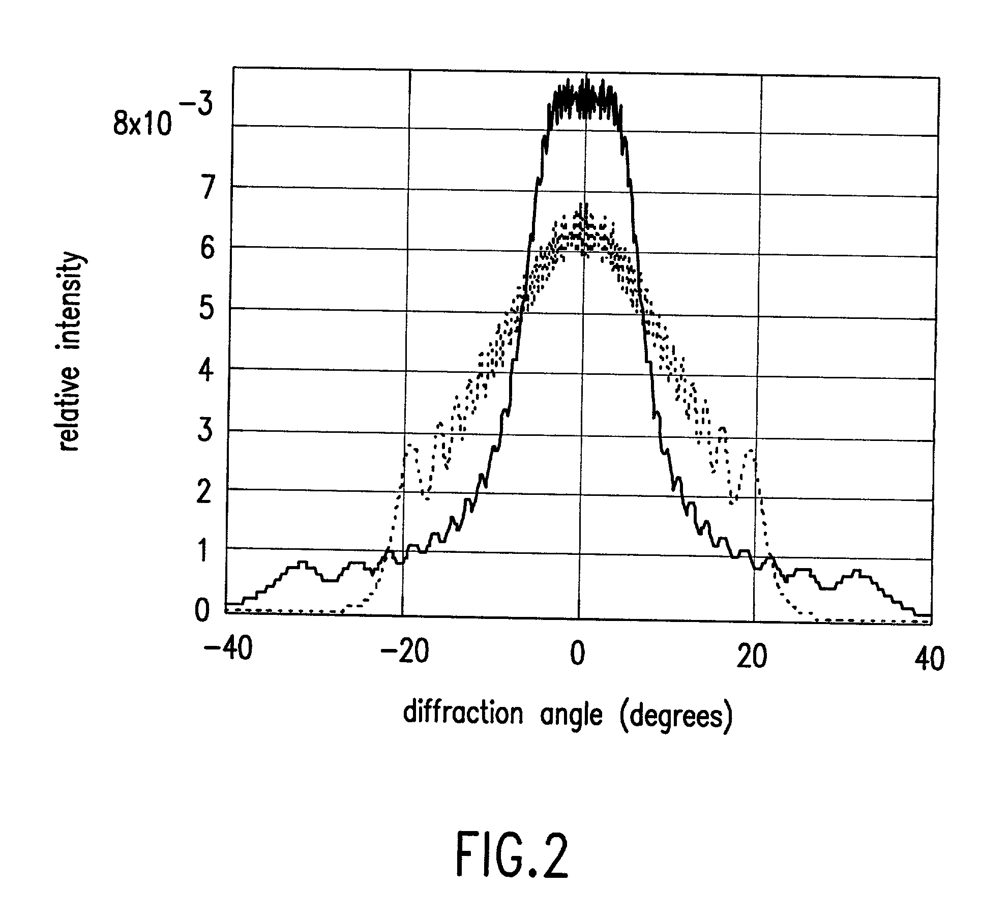
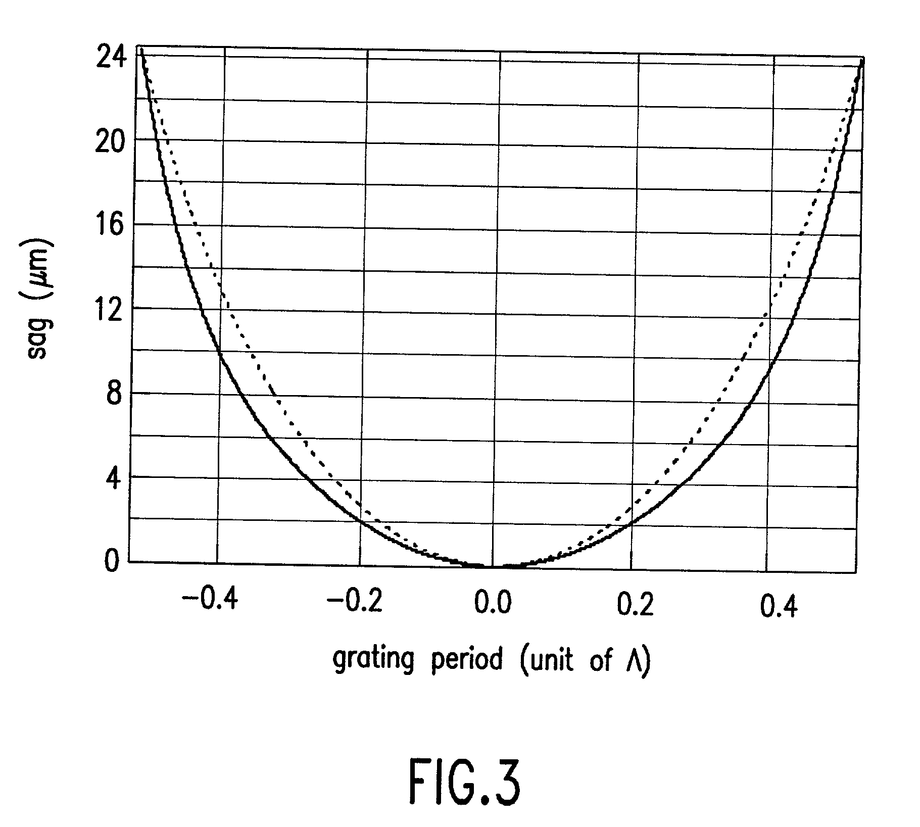
[0184] Consider initially a screen made of silicon to operate in the infrared in a wavelength range from 2 to 4 microns. FIG. ...
example 2
Effect of Vertical Offset
[0192] As illustrated in Example 1, the microstructure profile basically determines the shape and the divergence span of the scattering pattern. Randomizing the profile helps reduce the high-frequency oscillations and attain a smoother pattern. Depending on the spectral band of operation, hot spots may occur that are detrimental to the performance of the screen (see, for example, FIG. 26).
[0193] An important element useful in homogenizing the scattering pattern and providing a further parameter to help decrease the influence of hot spots is the vertical offset or piston of the microlens. Its effect is basically to displace a microlens along its axis of symmetry by a definite quantity. The net result is that the relative position of the vertex or origin of a microstructure varies as a function of its position on the screen.
[0194] To illustrate the effect, we again consider the array used to generate FIG. 26, that is, spherical microlenses of diameter 100 micr...
example 3
Spatial Arrangement of Microstructures
[0197] A defining global parameter of great relevance to the scattering pattern is the spatial arrangement of the microstructures on the screen. The main influence of the spatial arrangement is reflected in the overall symmetry of the scattering pattern.
[0198] For instance, the regular square array of FIG. 36 generates a three-dimensional pattern that resembles a rectangle, depending on the divergence angles introduced by the local configuration of the microlenses. The hexagonal array of FIG. 37, on the other hand, generates a scattering pattern in the form of a hexagon which can be stretched along one direction more than another depending on the divergence angles introduced by the configuration of the microlenses.
[0199] Apart from geometrical considerations, the overall symmetry is important in many aspects, but mainly because it affects how energy is concentrated in the observation plane. For instance, for a pattern of similar spatial extensio...
PUM
 Abstract
Description
Claims
Application Information
 - R&D
- Intellectual Property
- Life Sciences
- Materials
- Tech Scout
- Unparalleled Data Quality
- Higher Quality Content
- 60% Fewer Hallucinations
Browse by: Latest US Patents, China's latest patents, Technical Efficacy Thesaurus, Application Domain, Technology Topic, Popular Technical Reports.
© 2025 PatSnap. All rights reserved.Legal|Privacy policy|Modern Slavery Act Transparency Statement|Sitemap|About US| Contact US: help@patsnap.com


