Method of time multiplexing a programmable logic device

Inactive Publication Date: 2002-01-24
XILINX INC
View PDF0 Cites 295 Cited by
  • Summary
  • Abstract
  • Description
  • Claims
  • Application Information

AI Technical Summary

Problems solved by technology

However, due to the limited number of input/output connections, i.e. pins, between the FPGAs, not all circuits can be implemented using this approach.
Moreover, using more than one FPGA undesirably increases power consumption, cost, and space to implement the user circuit design.
However, for any given semiconductor fabrication technology, there are limitations

Method used


Image

  • Method of time multiplexing a programmable logic device
  • Method of time multiplexing a programmable logic device
  • Method of time multiplexing a programmable logic device

Examples


second embodiment

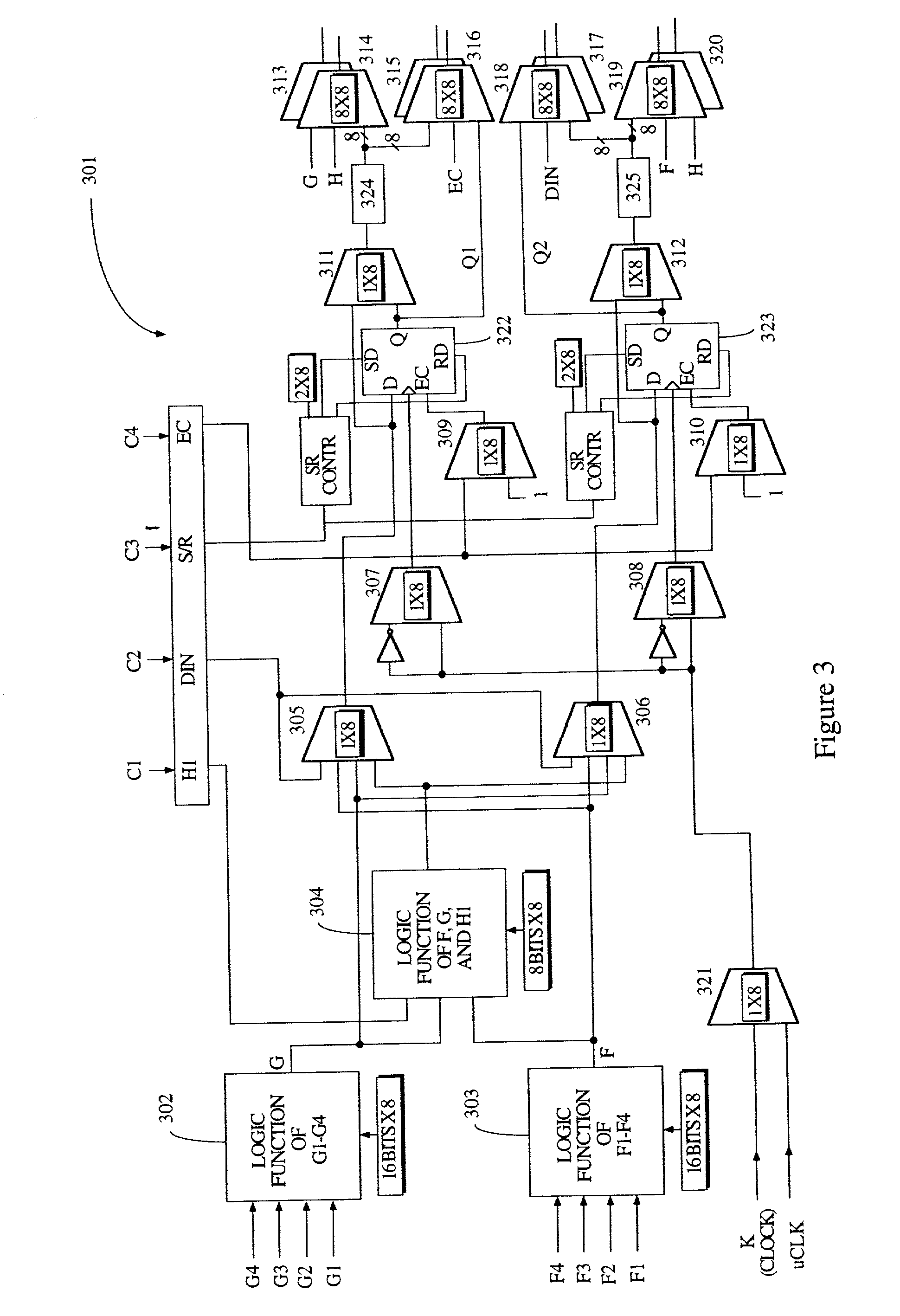
[0116] Micro registers 324 and 325 (FIG. 3) are located in alternative places. In one embodiment (shown in FIG. 3), micro registers 324, 325 are coupled to the input terminals of output multiplexers 313-320. In a second embodiment, the micro registers are coupled to the input terminals of logic function generators 302 and 303. If, for example, micro register 324 is coupled to the input terminals of logic function generator 302, then multiplexers 313-316 are simplified. Note that if two signals are generated in the same configuration and those signals are needed on the same pin of logic function generators on different configurations, a conflict arises. Specifically, if the micro registers are coupled to the input terminals of the logic function generators, two signals provided to those micro registers cannot be provided on the same configuration.

third embodiment

[0117] In a third embodiment, the micro registers are located in the interconnect, wherein signals are routed to the micro registers when available and routed from the micro registers when needed. In one instance, the micro registers are assigned independently of the logic function generators doing the calculation. In this manner, a placement program can automatically select only those micro registers having no conflict. This embodiment provides maximum flexibility as to data storage location.

fourth embodiment

[0118] In a fourth embodiment, the micro registers are located in a storage location independent of the configuration. The address or part of the address may be configuration bits or placement location. In this manner, only those values to be kept are stored and only locations that have no conflict are selected.

[0119] 2.2 Bus Hierarchy

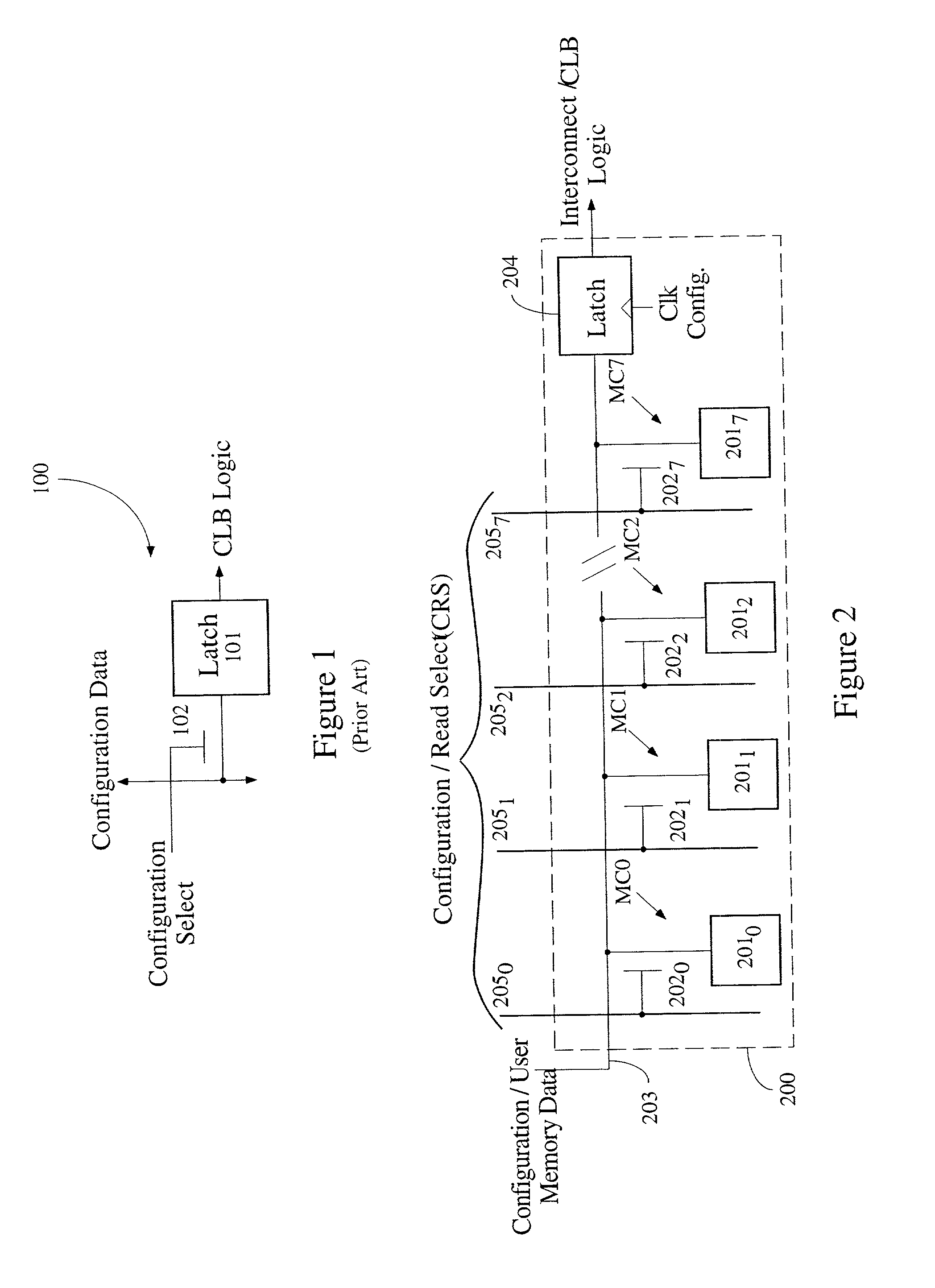
[0120] As described above in the Description of the Related Art, each configuration operation in a prior art FPGA is controlled by a set of configuration memory bits. The busses used to load these configuration bits typically form a single level of hierarchy, with vertical address lines spanning the full height of the CLB array, and horizontal data lines (referred to as a global bus) spanning the full array width.

[0121] In accordance with the present invention, each of the prior art configuration memory bits is replaced by N bits. Those N bits, i.e. the bits stored in memory cells MC0-MC7, are connected via their local busses 203 through switches 700 t...


PUM


Abstract

A programmable logic device (PLD) comprises at least one configurable element, and a plurality of programmable logic elements for configuring the configurable element(s). Alternatively, a PLD comprises an interconnect structure and a plurality of programmable logic elements for configuring the interconnect structure. In either embodiment, at least one of the programmable logic elements includes N memory cells. A predetermined one of the N memory cells forms part of a memory slice, wherein at least a portion of each slice of the programmable logic device is allocated to either configuration data or user data memory. Typically, one memory slice provides one configuration of the programmable logic device. In accordance with one embodiment, a memory access port is coupled between at least one of the N memory cells and either one configurable element or the interconnect, thereby facilitating loading of new configuration data into other memory slices during the one configuration. The new configuration data may include off-chip or on-chip data. The present invention typically allocates at least one slice to user data memory and includes means for disabling access to at least one of the N memory cells.

Description

CROSS REFERENCES TO RELATED APPLICATION[0001] This application is a continuation application of U.S. patent application Ser. No. 09 / 363,940, which was filed on Jul. 29, 1999.[0002] 1. Field of the Invention[0003] This invention relates generally to a programmable logic device, and in particular to a field programmable gate array in which the configurable logic blocks and the programmable routing matrices are reconfigured dynamically.[0004] 2. Description of Related Art[0005] Programmable logic devices such as field programmable gate arrays ("FPGAs") are a well known type of integrated circuit and are of wide applicability due to the flexibility provided by their reprogrammable nature. An FPGA typically includes an array of configurable logic blocks (CLBs) that are programmably interconnected to each other to provide logic functions desired by a user (a circuit designer). An FPGA typically includes a regular array of identical CLBs, wherein each CLB is individually programmed to perf...

Claims


Application Information

Patent Timeline
IPC IPC(8): G06F17/50G11C5/00H03K19/177
CPCG06F17/5054H03K19/17752H03K19/17756H03K19/1776H03K19/17776H03K19/17758G06F30/34
Inventor TRIMBERGER, STEPHEN M.CARBERRY, RICHARD A.JOHNSON, ROBERT ANDERSWONG, JENNIFER
Owner XILINX INC
Why Eureka
Try Eureka