Probe card and a method of manufacturing the same
a technology of probe card and manufacturing method, which is applied in the field of probe card, can solve the problems of faulty parts of the probe, the number of pins and the cost, and the inability to meet the requirements of this requirement,
- Summary
- Abstract
- Description
- Claims
- Application Information
AI Technical Summary
Problems solved by technology
Method used
Image

Examples
Embodiment Construction
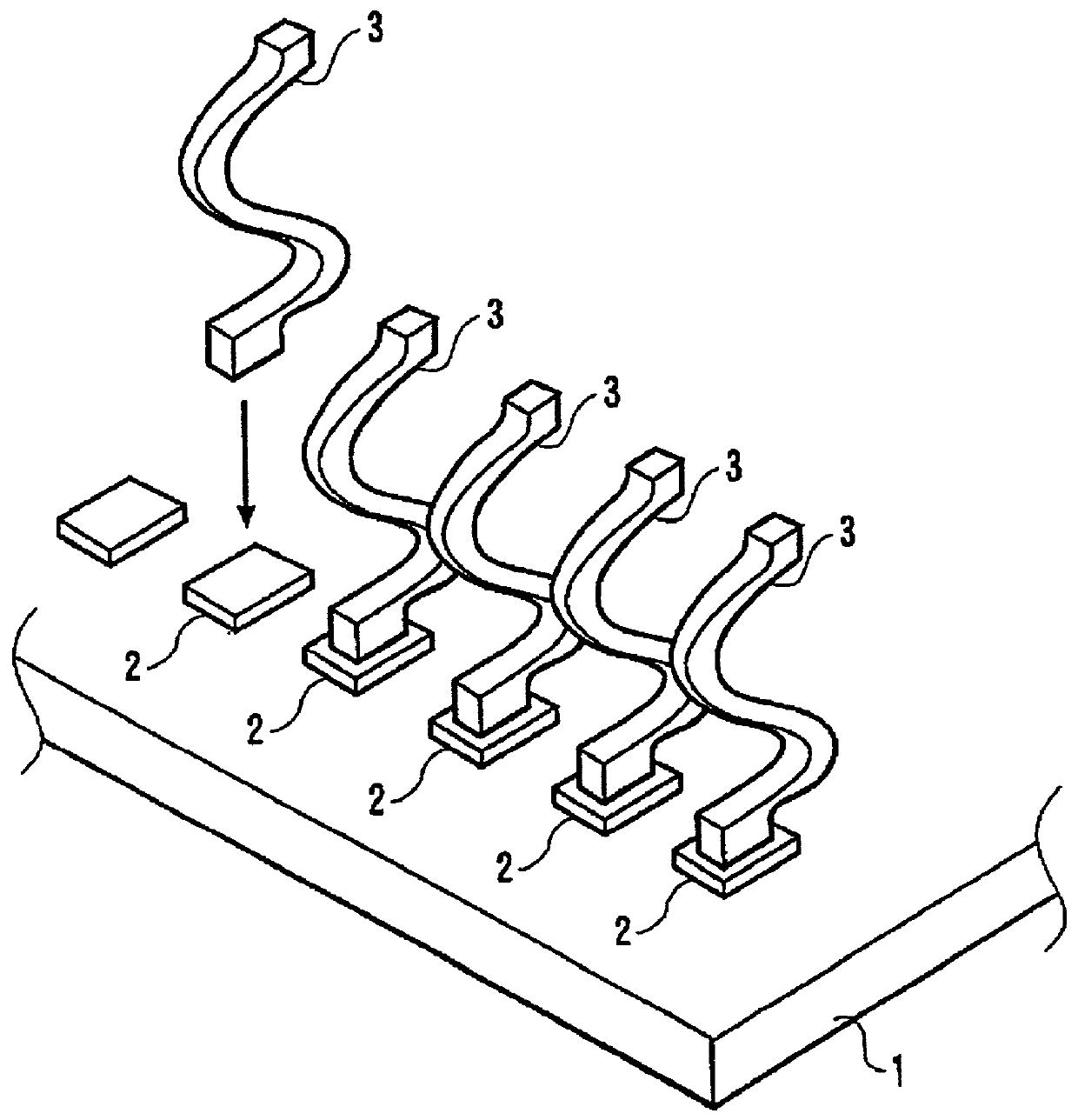
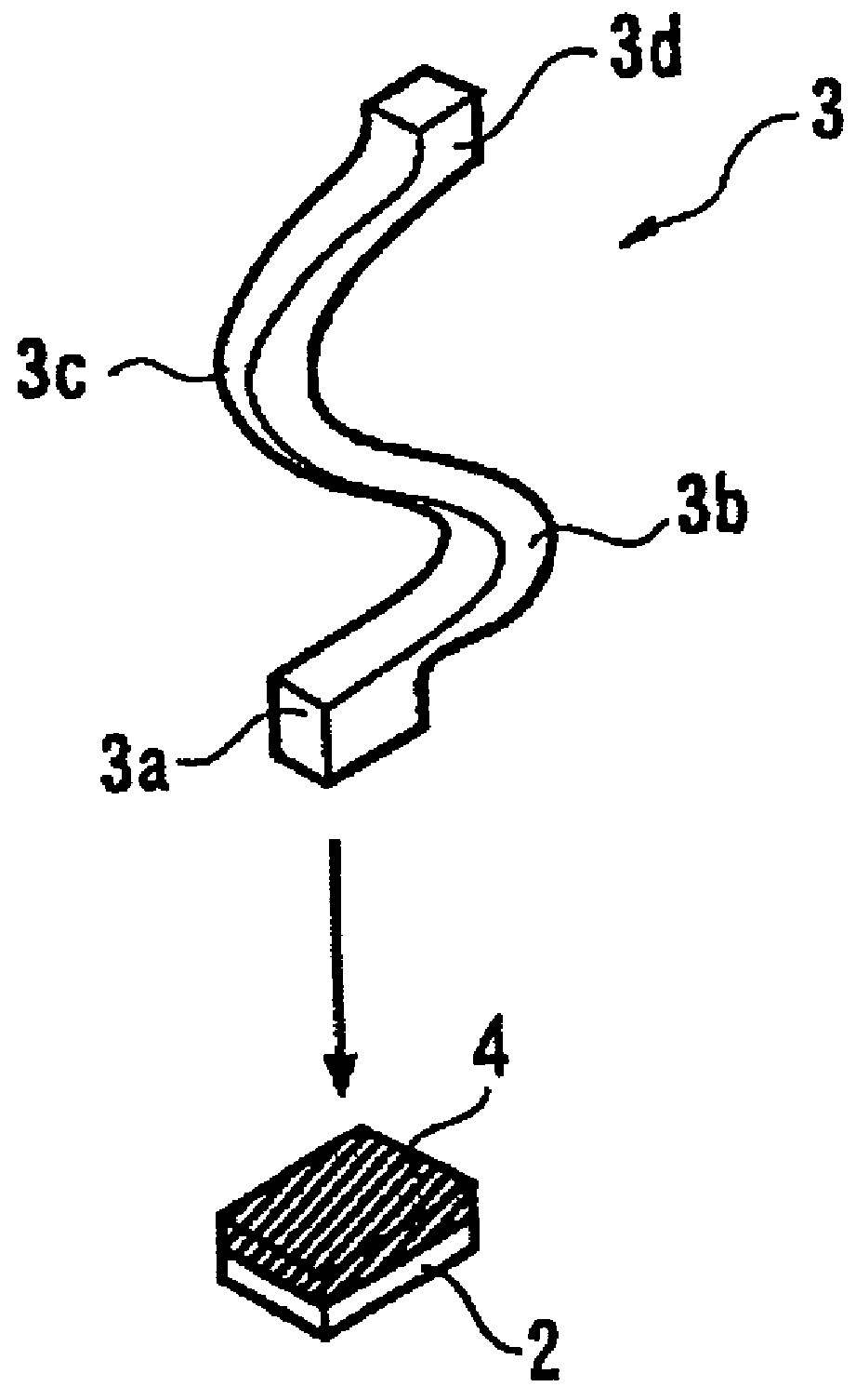
[0032] A probe card and a method of manufacturing the same according to a preferred embodiment of the invention are described with reference to FIGS. 1 and 2. FIG. 1 is a partially perspective view showing a probe card as an example to which the invention is applied. FIG. 2 is a view showing a step of jointing probes to the probe card in FIG. 1. In these figures, depicted by 1 is a wiring board (wiring means), 2 is pads (junction sections), 3 is probes (connection members) and 4 is solder.
[0033] The wiring board 1 has a plurality of wires (leads) so as to apply a power supply voltage, a signal and so forth to a plurality of semiconductor integrated circuits at the same time for testing excitation of the semiconductor integrated circuits formed on a semiconductor wafer. Further, a plurality of (e.g., several thousands of) pads 2 are formed on the surface of the wiring board 1 as shown in FIG. 1, wherein respective wires are connected to corresponding pads 2 so that the excitation tes...
PUM
 Abstract
Description
Claims
Application Information
 - R&D
- Intellectual Property
- Life Sciences
- Materials
- Tech Scout
- Unparalleled Data Quality
- Higher Quality Content
- 60% Fewer Hallucinations
Browse by: Latest US Patents, China's latest patents, Technical Efficacy Thesaurus, Application Domain, Technology Topic, Popular Technical Reports.
© 2025 PatSnap. All rights reserved.Legal|Privacy policy|Modern Slavery Act Transparency Statement|Sitemap|About US| Contact US: help@patsnap.com