
Hybrid semiconductor photodetector assembly

a photodetectors and hybrid technology, applied in the field of photodetectors, can solve the problems of reducing the response time and the capacitance of the junction, and achieve the effects of reducing the cost factor of conventional ingaas photodetectors, high performance, and high performan

Active Publication Date: 2022-04-19
ANALOG DEVICES INC
View PDF40 Cites 0 Cited by
  • Summary
  • Abstract
  • Description
  • Claims
  • Application Information

AI Technical Summary

Benefits of technology

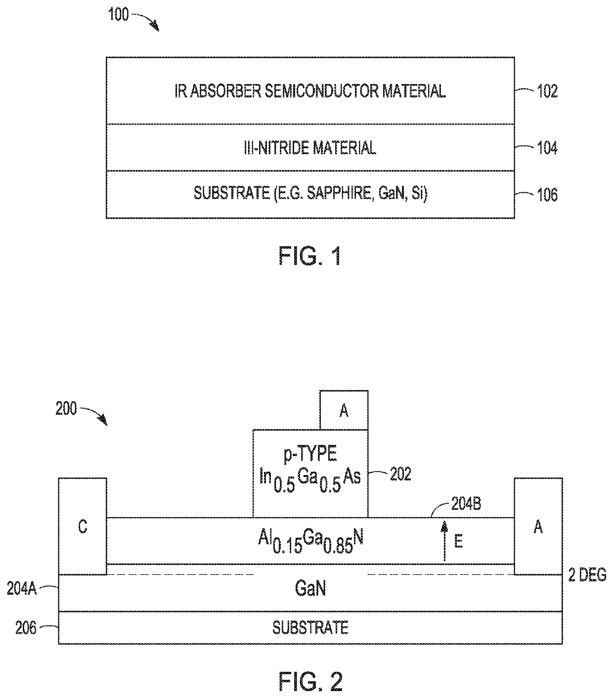
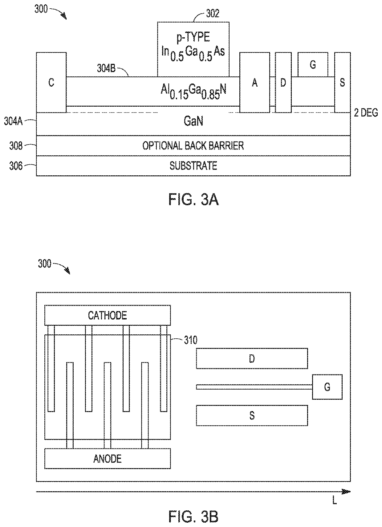
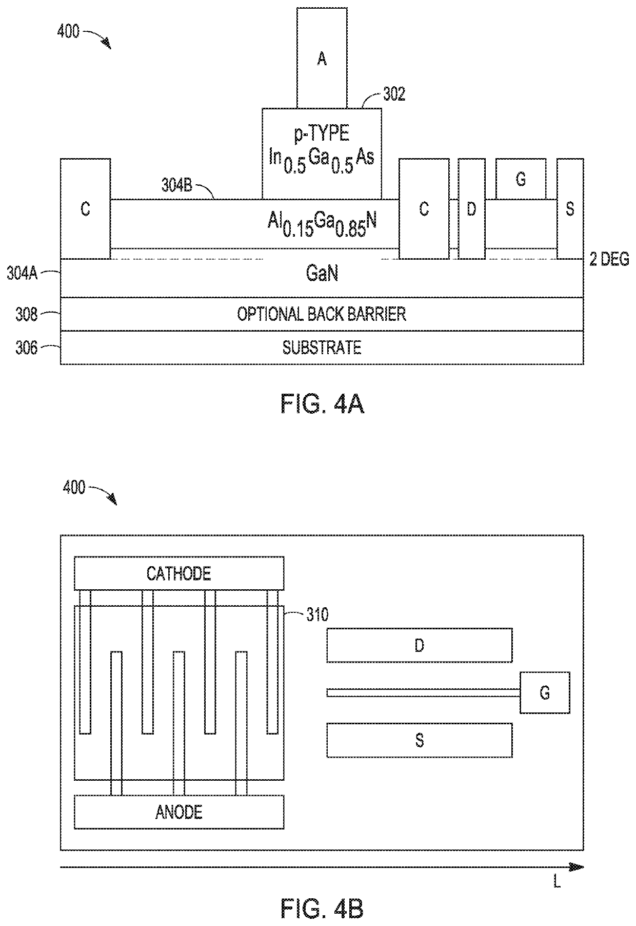
This disclosure describes a way to make an inexpensive IR photodetector that works well in short-wave infrared applications like LIDAR. It can be made into a photodiode, a phototransistor, or a hybrid of both. This hybrid detector is cheaper than conventional InGaAs detectors, but still performs well in SWIR applications. Overall, this disclosure provides a way to get a high-performing, affordable detector for IR applications.

Problems solved by technology

This can reduce the response time because the additional reverse bias can increase the width of the depletion layer, which can decrease the junction's capacitance.

Method used


Image

  • Hybrid semiconductor photodetector assembly
  • Hybrid semiconductor photodetector assembly
  • Hybrid semiconductor photodetector assembly

Examples


Embodiment Construction

[0040]Photodetectors can be combined into image sensing devices, such as focal plane arrays (FPAs), and used in numerous automobile, space, and military applications. For example, one application includes remote sensing using light pulses emitted for example by lasers and reflected by distant objects can be referred to as LIDAR (light detection and ranging). A LIDAR receiver can include an optical receiver having a photodiode (PD) as a receiving element, and a transimpedance amplifier (TIA), for example a shunt-feedback amplifier, which converts the photocurrent from the receiving photodiode into a voltage.

[0041]LIDAR systems can use short-wave infrared light (SWIR), such as wavelengths greater than about 1 micrometer (μm) to about 3 μm. In these applications, conventional photodetectors use indium gallium arsenide (InGaAs), photodiode (PDs) for achieving high performance at a wavelength of about 1.5 μm. However, the high cost of InGaAs PDs have delayed their adoption in different c...


PUM

PropertyMeasurementUnit
wavelengthsaaaaaaaaaa

Abstract

An inexpensive IR photodetector assembly that can provide high performance in SWIR applications, such as LIDAR. The photodetector assembly can operate as a photodiode, a phototransistor, or can include both a photodiode and a phototransistor. The hybrid photodetector can be composed of one or more absorber layer materials from a first semiconductor family, e.g., p-type InGaAs, laying on one or more wide-band gap semiconductor transducer layer materials from a second semiconductor family, e.g., aluminum gallium nitride (AlGaN) and gallium nitride (GaN), or AlGaN / n-GaN. As such, the absorber layer material and the wide band gap materials can be from two different semiconductor families, making the IR photodetector a hybrid of semiconductor families. After shining IR light onto the absorber layer material, the photo-generated electron-hole pairs can be collected as photocurrent in the photo-voltaic mode.

Description

CLAIM OF PRIORITY[0001]This application claims the benefit of priority of U.S. Provisional Patent Application Ser. No. 62 / 782,914, titled “HYBRID SEMICONDUCTOR PHOTODETECTOR ASSEMBLY” to Mohamed Azize, filed on Dec. 20, 2018, the entire contents of which being incorporated herein by reference.FIELD OF THE DISCLOSURE[0002]This document pertains generally, but not by way of limitation, to photodetector assemblies and methods.BACKGROUND[0003]A photodiode is typically a PN junction or PIN structure. When a photon of sufficient energy strikes the diode, it can create an electron-hole pair. This mechanism is also known as the inner photoelectric effect. If the absorption occurs in the junction's depletion region, or one diffusion length away from it, these carriers are swept from the junction by the built-in electric field of the depletion region. Thus, holes move toward the anode, and electrons move toward the cathode, and a photocurrent is produced.[0004]When used in zero bias or photov...

Claims


Application Information

Patent Timeline
Patent Type & Authority Patents(United States)
IPC IPC(8): H01L31/101H01L31/112H01L31/0304H01L31/18H01L31/109H01L29/778
CPCH01L31/1129H01L29/7786H01L31/03046H01L31/109H01L31/1844H01L31/1856H01L31/03044H01L31/112Y02E10/544
Inventor AZIZE, MOHAMED
Owner ANALOG DEVICES INC
Learn More