Power conversion device

Active Publication Date: 2021-09-21
MITSUBISHI ELECTRIC CORP
View PDF10 Cites 0 Cited by
  • Summary
  • Abstract
  • Description
  • Claims
  • Application Information

AI Technical Summary

Benefits of technology

The power conversion device described in this patent reduces the number of electrical conductors that touch, which reduces the risk of surge voltage during operation. This is achieved by arranging the conductors in a way that they don't overlap each other, which decreases the amount of capacitance between them. This design reduces the size of the device and ensures better insulation.

Problems solved by technology

However, electric vehicles have no engine as a drive source, and hence, as a matter of course, an alternator to be driven by an engine cannot be used.
Further, hybrid vehicles employ a start-stop system (system for automatically stopping the engine when the vehicle is stopped, for example, when the vehicle waits for a traffic light at an intersection) in order to improve fuel efficiency and reduce exhaust gas, and hence, also in this case, an alternator cannot be used.
In this case, in a case of turning off the switching elements, when a wiring inductance component is large, a surge voltage may be increased, and the surge voltage may damage the switching elements.

Method used


Image

  • Power conversion device
  • Power conversion device
  • Power conversion device

Examples


first embodiment

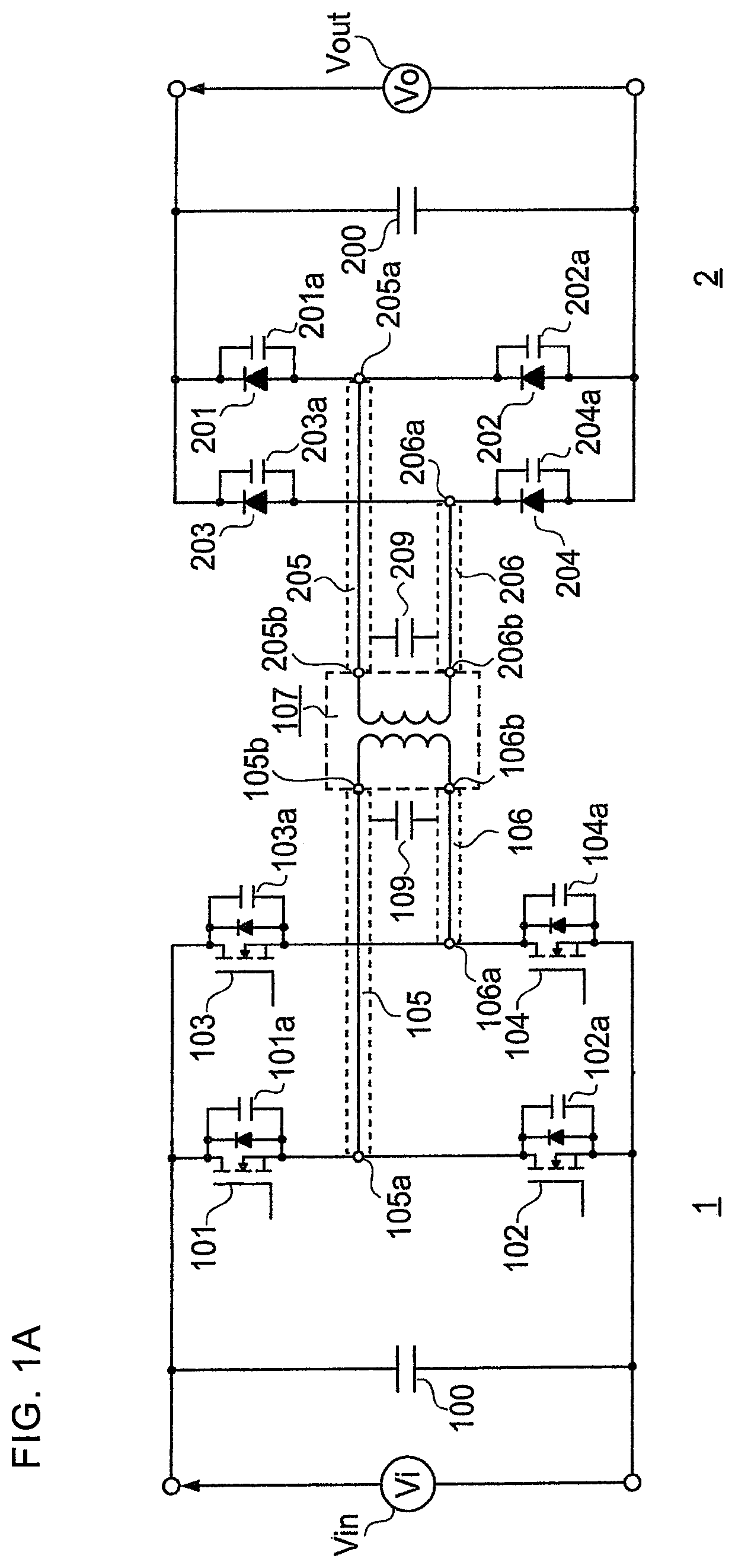
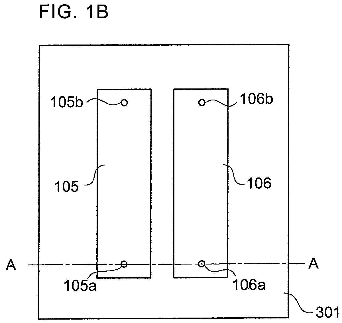
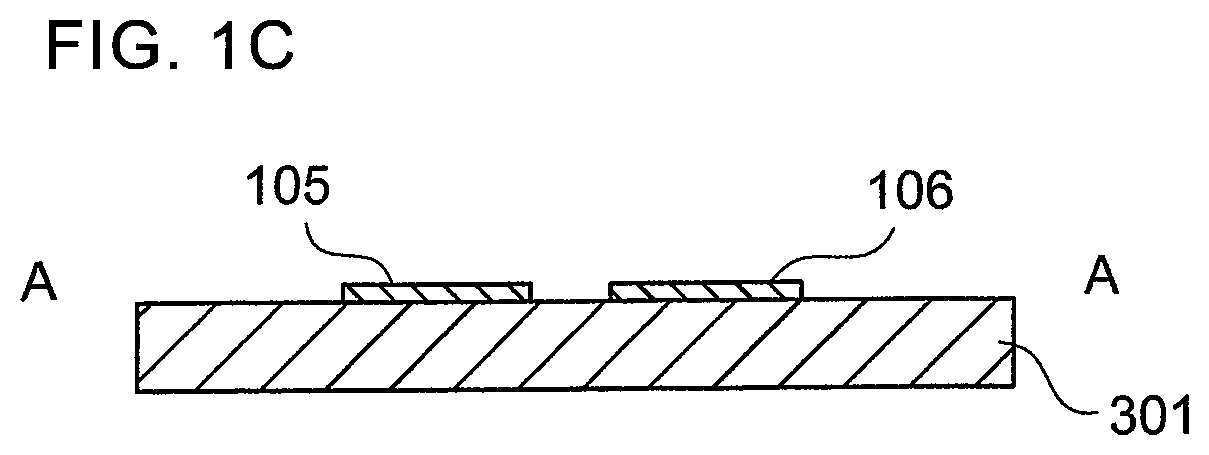
[0053]FIG. 1A is a configuration diagram for illustrating a circuit configuration of a power conversion device according to a first embodiment of the present invention. Further, FIG. 1B is a plan view for illustrating configurations of a first conductor and a second conductor formed in the power conversion device according to the first embodiment of the present invention, and FIG. 1C is an A-A sectional view of FIG. 1B.

[0054]As illustrated in FIG. 1A, the power conversion device includes a primary circuit 1, a secondary circuit 2, and an isolation transformer 107 formed between the primary circuit 1 and the secondary circuit 2.

[0055]The primary circuit 1 includes an input capacitor 100, a first switching element 101, a second switching element 102, a third switching element 103, and a fourth switching element 104. The input capacitor 100 is connected in parallel to the subsequent stage of an input voltage Vin. Further, the first switching element 101 has a parasitic capacitance 101a...

second embodiment

[0084]The overall configuration of a power conversion device according to a second embodiment of the present invention is the same as the above-mentioned configuration of the first embodiment illustrated in FIG. 1A.

[0085]FIG. 4A to FIG. 4D are schematic configuration views for illustrating configurations of the first conductor 105 and the second conductor 106 formed in the power conversion device according to the second embodiment of the present invention. In the above-mentioned first embodiment, as illustrated in FIG. 1B and FIG. 1C, the first conductor 105 and the second conductor 106 are wired on one surface of the insulating substrate 301. In the second embodiment, as illustrated in FIG. 4A to FIG. 4D, the first conductor 105 and the second conductor 106 are wired on both surfaces of the insulating substrate 301.

[0086]Further, the first conductors 105 wired on both the surfaces of the insulating substrate 301 are electrically connected to each other via through holes 105t1 and 1...

third embodiment

[0098]The overall configuration of a power conversion device according to a third embodiment of the present invention is the same as the above-mentioned configuration of the first embodiment illustrated in FIG. 1A.

[0099]FIG. 5A to FIG. 5D are schematic configuration views for illustrating configurations of the first conductor 105 and the second conductor 106 formed in the power conversion device according to the third embodiment of the present invention. In the above-mentioned second embodiment, the insulating substrate 301 is formed of a single layer, and the first conductor 105 and the second conductor 106 are each wired in two layers. In contrast, in the third embodiment, the insulating substrate 301 is formed of two or more layers, and the first conductor 105 and the second conductor 106 are also each wired in two or more layers. That is, in the third embodiment, as illustrated in FIG. 5A to FIG. 5D, a plurality of insulating substrates 301 are laminated. Further, on the upper s...


PUM


Abstract

Provided is a power conversion device including: an isolation transformer (107) including a first winding and a second winding; switching elements (101 to 104) to be connected to the first winding of the isolation transformer (107); a first conductor (105) configured to connect one end of the first winding of the isolation transformer (107) to the switching elements (101 and 102); and a second conductor (106) configured to connect another end of the first winding of the isolation transformer (107) to the switching elements (103 and 104), the first conductor (105) and the second conductor (106) being arranged on an insulating substrate (301) so as to be parallel to each other so that the first conductor (105) and the second conductor (106) are prevented from overlapping each other.

Description

CROSS REFERENCE TO RELATED APPLICATIONS[0001]This application is a National Stage of International Application No. PCT / JP2017 / 037715 filed Oct. 18, 2017, claiming priority based on Japanese Patent Application No. 2017-131035 filed Jul. 4, 2017.TECHNICAL FIELD[0002]The present invention relates to a power conversion device, and more particularly, to a power conversion device including semiconductor switching elements and an isolation transformer.BACKGROUND ART[0003]Electric vehicles and hybrid vehicles include, similarly to motor vehicles powered by an engine, an auxiliary battery for a control circuit configured to operate electrical components. However, electric vehicles have no engine as a drive source, and hence, as a matter of course, an alternator to be driven by an engine cannot be used. Further, hybrid vehicles employ a start-stop system (system for automatically stopping the engine when the vehicle is stopped, for example, when the vehicle waits for a traffic light at an int...

Claims


Application Information

Patent Timeline
IPC IPC(8): H02M3/335H02M3/00H05K1/03H01F27/32H02M7/00
CPCH02M3/33592H01F27/32H02M3/003H02M3/33523H02M7/003H05K1/0306Y02B70/10H05K1/115H05K1/165H02M1/0064
Inventor YABUUCHI, NAOYA
Owner MITSUBISHI ELECTRIC CORP
Why Eureka
Try Eureka