


Quick Research
Generate reliable direction feasibility study reports for your R&D in just a few steps.

Technical Q&A
Discover and master advanced knowledge NOW. Basics, ideas, possibilities, all at once.

Find Solutions
As an expert in R&D theories, this can generate solutions to your technical problems instantly.

Evaluate Feasibility
Analyze your overall solution with one click, know your potential R&D risks in advance.

Monitor Landscape
Get weekly tech updates, stay abreast of the latest tech innovations and key insights.
Semiconductor device and method of manufacturing the same
a semiconductor device and semiconductor technology, applied in the direction of semiconductor devices, electrical devices, transistors, etc., can solve the problems of difficult miniaturization of semiconductor devices, achieve the effect of reducing surface field, improving breakdown voltage, and not increasing chip siz
- Summary
- Abstract
- Description
- Claims
- Application Information
AI Technical Summary
Benefits of technology
Problems solved by technology
Method used
Image

Examples
first embodiment
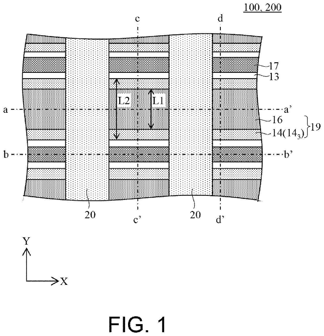
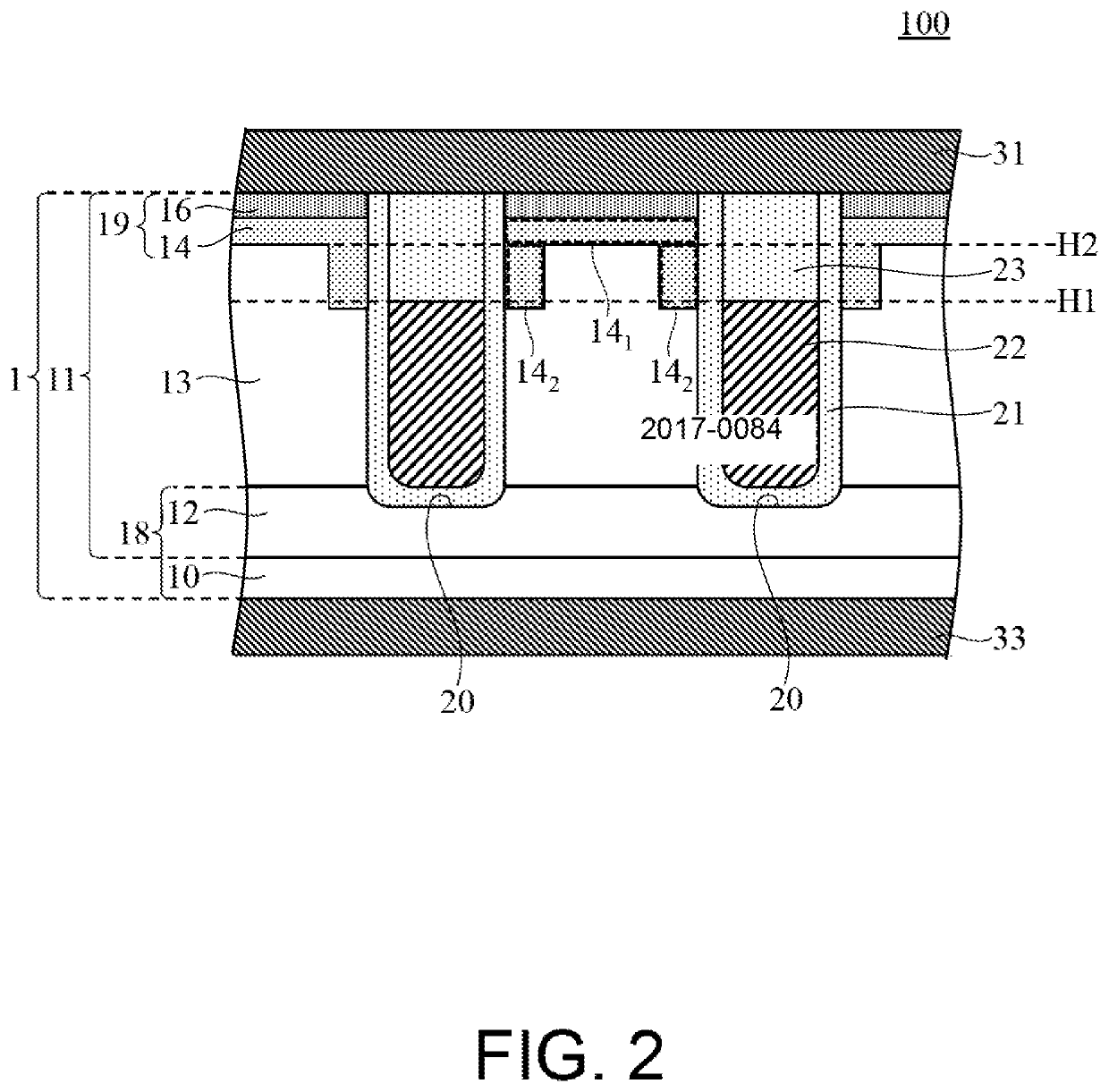
[0047]As described above, in the first embodiment, the source region 19 includes the source portion 16 and the source portion 14 having an impurity concentration lower than that of the source portion 16. The source portion 14 having a low impurity concentration has a structure (RESURF structure) to include the first sub-portion 141 and the second sub-portions 142. The first sub-portion 141 has the depth from the bottom surface of the source portion 16 up to the height H2 which is higher than the height H1 as the height of the upper surface of the gate electrode 22. The second sub-portion 142 includes the upper surface in contact with the part of the bottom surface of the first sub-portion 141, the one side surface in the X-direction perpendicular to the extending direction (Y-direction) of the trench 20 in contact with the outer side surface of the trench 20, and the another surface in the X-direction, the both side surfaces in the Y-direction and the bottom surface in contact with ...
second embodiment
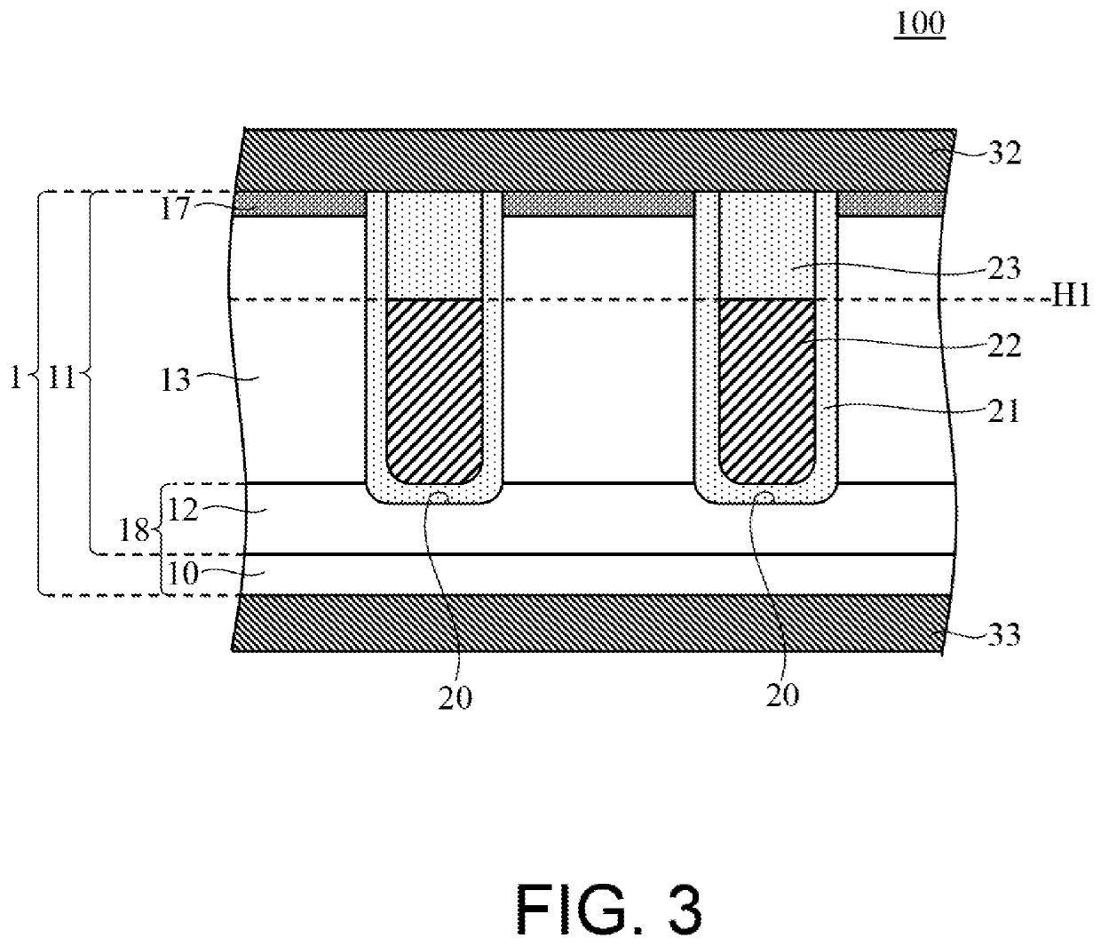
[0048]Next, a semiconductor device 200 including a vertical MOSFET according to the present invention is described with reference to FIG. 1 and FIG. 6. FIG. 6 is a sectional view taken along the line a-a′ of FIG. 1.
[0049]In the semiconductor device 200 according to the second embodiment, the structure of the drain region 18 is different from that of the semiconductor device 100 according to the first embodiment. Other components are identical to those of the semiconductor device 100, and hence the same components are denoted by the same reference numerals, and redundant description is omitted as appropriate.
[0050]The drain region 18 in the semiconductor device 200 of the second embodiment includes an N-type third drain portion 15 in addition to the semiconductor substrate 10 and the semiconductor layer 12, respectively referred to as the first drain portion and the second drain portion. The third drain portion 15 is formed to extend to the semiconductor layer 12 and the base layer 1...
PUM
| Property | Measurement | Unit |
|---|---|---|
| conductivity | aaaaa | aaaaa |
| thickness | aaaaa | aaaaa |
| insulating | aaaaa | aaaaa |
Abstract
Description
Claims
Application Information
 - R&D Engineer
- R&D Manager
- IP Professional
- Industry Leading Data Capabilities
- Powerful AI technology
- Patent DNA Extraction
Browse by: Latest US Patents, China's latest patents, Technical Efficacy Thesaurus, Application Domain, Technology Topic, Popular Technical Reports.
© 2024 PatSnap. All rights reserved.Legal|Privacy policy|Modern Slavery Act Transparency Statement|Sitemap|About US| Contact US: help@patsnap.com