
Input device manufacturing method

a manufacturing method and input device technology, applied in the field of input device manufacturing methods, can solve the problems of loss of smoothness of the front surface of the input device, and achieve the effects of reducing the number of steps

Active Publication Date: 2020-05-12
ALPS ALPINE CO LTD
View PDF6 Cites 0 Cited by
  • Summary
  • Abstract
  • Description
  • Claims
  • Application Information

AI Technical Summary

Benefits of technology

The present invention provides an input device manufacturing method that can improve the smoothness of the front surface of the input device by restraining concave and convex parts from appearing on it. This is achieved by a method that can mitigate a step formed due to the thickness of the sensor film or a difference in thermal contraction caused between different members and have the adhesive layer of the decorative film suppress the step or difference. The sensor film is insert-molded in the adhesive layer, which can burry flexible printed circuit board, wires, and other components in the resin layer to restrain them from breaking and improve the reliability of the input device. The edges of the sensor film are buried in the resin layer to suppress a step formed during the insert molding of the sensor film. The sensor film is only provided in the detection area, which can increase the number of sensor films that can be taken out in the manufacturing process. The terminal part of a lead wire provided on the non-detection area can be exposed from the main surface of the resin layer without excessively thinning the resin layer. The use of a three dimension overlay method can increase the tight contact of the decorative film with the sensor film and restrain concave and convex parts from appearing on the front surface of the input device.

Problems solved by technology

This is problematic in that the smoothness of the front surface of the touch sensor device is lost.

Method used


Image

  • Input device manufacturing method
  • Input device manufacturing method
  • Input device manufacturing method

Examples


Embodiment Construction

[0025]An embodiment of the present invention will be described below with reference the drawings. In the descriptions below, like elements will be denoted by like reference characters and repeated descriptions will be appropriately omitted for members that have been described once.

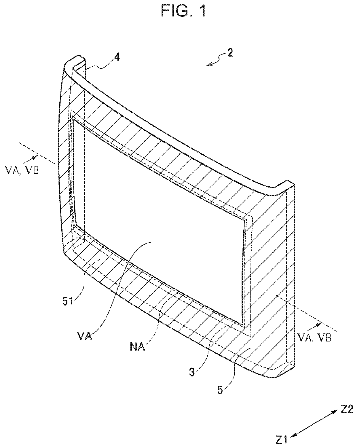
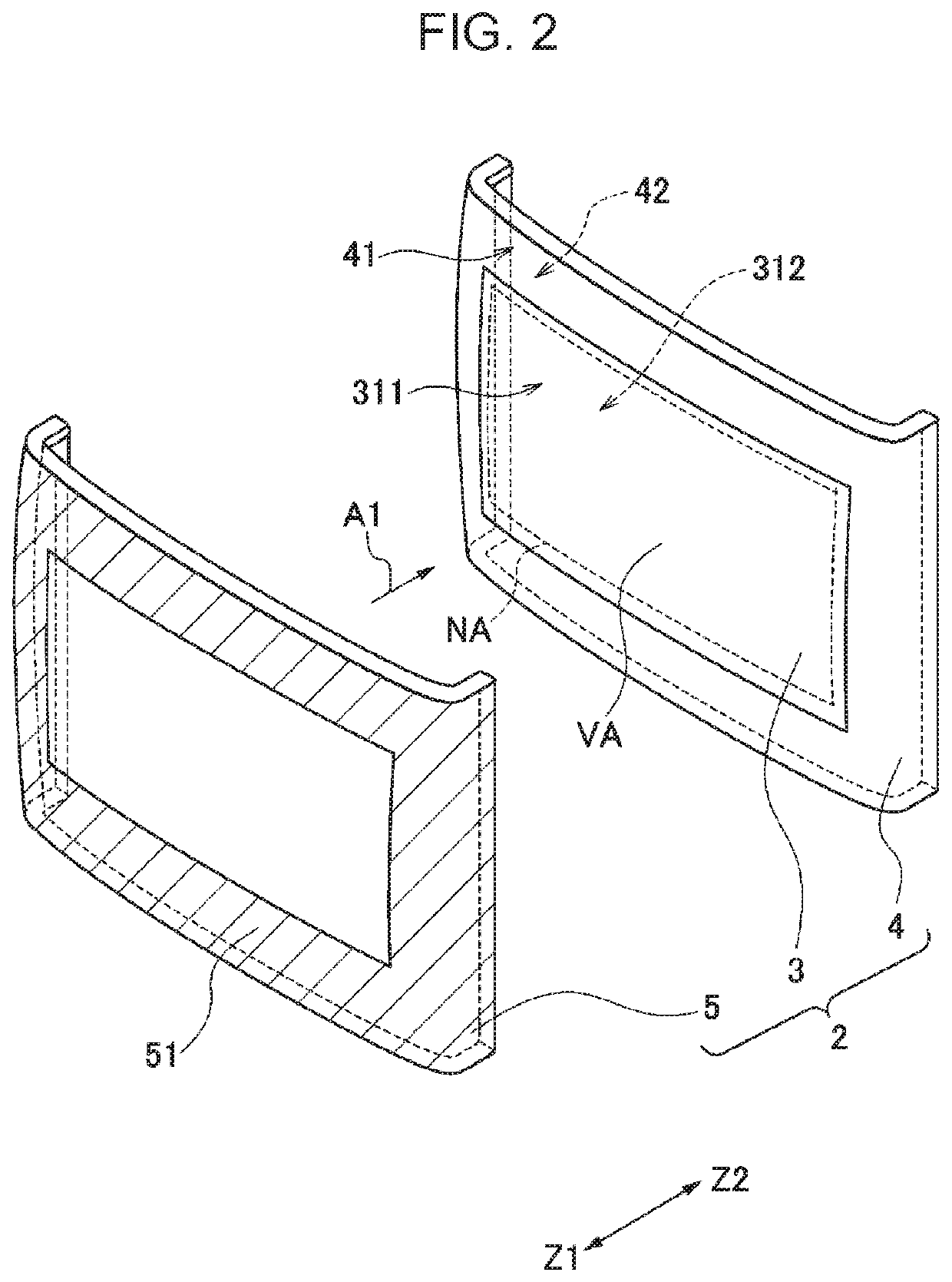
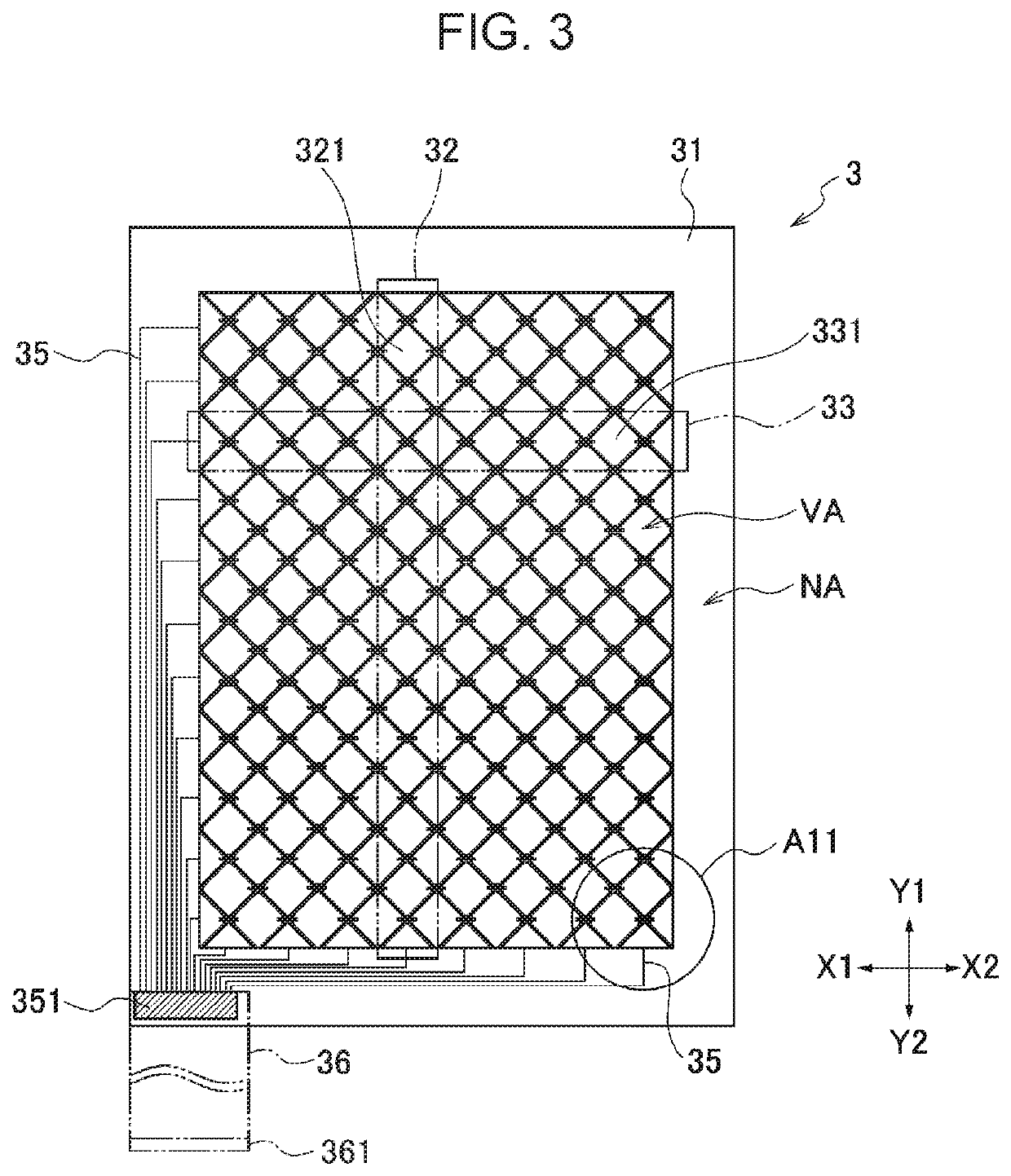
[0026]FIG. 1 is a perspective view illustrating an input device manufactured by a manufacturing method according to an embodiment of the present invention. FIG. 2 is an exploded view illustrating the input device manufactured by the manufacturing method according to the embodiment of the present invention. FIG. 3 is a plan view illustrating a sensor film in the embodiment of the present invention. FIG. 4 is an enlarged view in which the area A11 indicated in FIG. 3 is enlarged.

[0027]Before an input device manufacturing method according to this embodiment will be described, the input device manufactured by the manufacturing method will be described first. In the specification of this application, “transpare...


PUM

PropertyMeasurementUnit
visible light transmittanceaaaaaaaaaa
hazeaaaaaaaaaa

Abstract

An input device manufacturing method includes: a first process in which, in a state in which a sensor film is inserted into a die, the sensor film having a detection area and a non-detection area other than the detection area, the detection area and the non-detection area constituting the sensor, as well as a first surface formed into a curved surface and a second surface positioned opposite to the first surface, a material that includes a synthetic resin having a translucent property is poured into the die to form a resin layer on the same side as the second surface; and a second process in which a decorative film having a decorative area that covers the non-detection area is pasted to the first surface with an adhesive layer intervening between the decorative film and the first surface.

Description

CLAIM OF PRIORITY[0001]This application is a Continuation of International Application No. PCT / JP2017 / 035892 filed on Oct. 3, 2017, which claims benefit of Japanese Patent Application No. 2016-196436 filed on Oct. 4, 2016. The entire contents of each application noted above are hereby incorporated by reference.BACKGROUND OF THE INVENTION1. Field of the Invention[0002]The present invention relates to an input device manufacturing method, and more particularly to a method of manufacturing an input device provided with a sensor film having a two-dimensional or three-dimensional curved surface.2. Description of the Related Art[0003]In various information processing apparatuses, a translucent input device is placed at the front of a display panel such as a color liquid crystal panel. This type of input device is called a touch panel. In a touch panel, a capacitor is formed between electrodes and, when a finger of a person comes close to the touch panel, the coordinates of the close posit...

Claims


Application Information

Patent Timeline
Patent Type & Authority Patents(United States)
IPC IPC(8): G06F3/044G06F3/041
CPCG06F3/044G06F3/041G06F2203/04103G06F2203/04112G06F3/0446G06F3/0445G06F2203/04102
Inventor HASHIDA, JUNJI
Owner ALPS ALPINE CO LTD
Learn More