
Temperature compensation for unselected memory cells and string select switches in NAND flash memory

a temperature compensation and memory cell technology, applied in the field of flash memory, can solve problems such as reducing the sensing margin in the read operation, and achieve the effect of large margins

Active Publication Date: 2019-12-24
MACRONIX INT CO LTD
View PDF8 Cites 0 Cited by
  • Summary
  • Abstract
  • Description
  • Claims
  • Application Information

AI Technical Summary

Benefits of technology

This patent describes a memory device that uses temperature compensation to improve the performance of program and inhibit operations. The device includes word line drivers that provide low temperatures to unswitched memory cells and high temperatures to the selected cell for programming. A string select line voltage also compensates for temperature variations to provide larger margin for successful program and inhibit operations. Overall, this technology improves the reliability and efficiency of memory devices.

Problems solved by technology

Consequently the resistance of the NAND string and the current through the NAND string will vary due to the temperature dependency of unselected memory cells, and may reduce sensing margins in a read operation.

Method used


Image

  • Temperature compensation for unselected memory cells and string select switches in NAND flash memory
  • Temperature compensation for unselected memory cells and string select switches in NAND flash memory
  • Temperature compensation for unselected memory cells and string select switches in NAND flash memory

Examples


Embodiment Construction

[0033]The following description will typically be with reference to specific structural embodiments and methods. It is to be understood that there is no intention to limit the technology to the specifically disclosed embodiments and methods but that the technology may be practiced using other features, elements, methods and embodiments. Preferred embodiments are described to illustrate the present technology, not to limit its scope, which is defined by the claims. Those of ordinary skill in the art will recognize a variety of equivalent variations on the description that follows. Like elements in various embodiments are commonly referred to with like reference numerals.

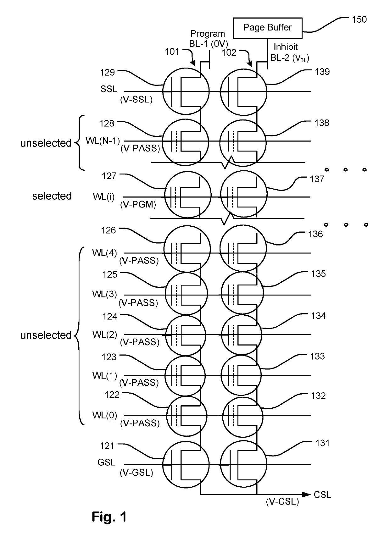
[0034]FIG. 1 is a circuit diagram showing part of a NAND array comprising a NAND string (e.g. 101) that includes a plurality of memory cells arranged in series in a semiconductor body. A memory cell (e.g. 127) in the NAND string can be selected, and other memory cells (e.g. 121-126, 128) in the NAND string can be unse...


PUM


Abstract

A memory device comprises a first NAND string that includes a first plurality of memory cells and a first string select switch arranged in series, the first string select switch disposed between a first bit line and a first end of the first plurality, a second NAND string that includes a second plurality of memory cells and a second string select switch arranged in series, the second string select switch disposed between a second bit line and a first end of the second plurality, word lines coupled to memory cells in the first plurality and memory cells in the second plurality, and a string select line coupled to the first and second string select switches. A method of operating such a memory device comprises applying a voltage varying in a manner complementary to absolute temperature to at least one of the word lines and the string select line.

Description

BACKGROUNDField[0001]The present invention relates to flash memory, and more particularly to operating flash memory in a NAND configuration.Description of Related Art[0002]In a NAND flash structure, a NAND string typically includes a string select transistor with its drain terminal connected to a bit line and its gate terminal connected to a string select line (SSL), and a ground select transistor with its source terminal connected to a common source line (CSL) and its gate terminal connected to a ground select line (GSL). Memory cells on the NAND string are between the string select transistor and the ground select transistor. Word lines are coupled to the gate terminals of the memory cells. In operation, one of the memory cells in a NAND string can be selected while other memory cells in the NAND string are unselected.[0003]The threshold voltages of the unselected memory cells in a NAND string vary along the NAND string depending on their data values stored, and in addition have t...

Claims


Application Information

Patent Timeline
Patent Type & Authority Patents(United States)
IPC IPC(8): G11C11/00G11C16/34G11C16/04G11C16/24G11C16/26G11C16/10G11C16/08
CPCG11C16/3427G11C16/08G11C16/0483G11C16/26G11C16/24G11C16/10G11C16/3436G11C7/04
Inventor YANG, YIH-SHANSHEN, SHIN-JANG
Owner MACRONIX INT CO LTD
Learn More