RAMO4 substrate and nitride semiconductor apparatus
a ramo4 substrate and nitride technology, applied in the direction of semiconductor lasers, crystal growth process, polycrystalline material growth, etc., can solve the problems of large lattice mismatch of scalmgosub>4 /sub>substrate, high defect density, and surface cleavage of scalmgosub>substrate, etc., to achieve satisfactory crystallinity and flatness, and higher performance
- Summary
- Abstract
- Description
- Claims
- Application Information
AI Technical Summary
Benefits of technology
Problems solved by technology
Method used
Image
Examples
embodiment 1
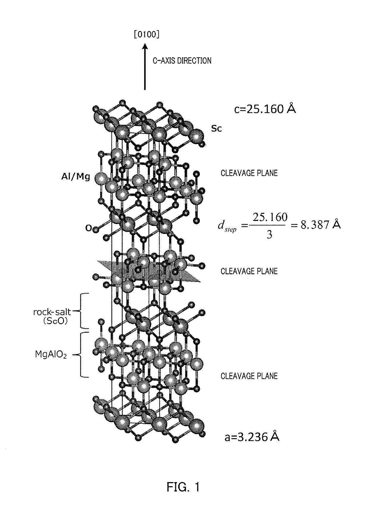
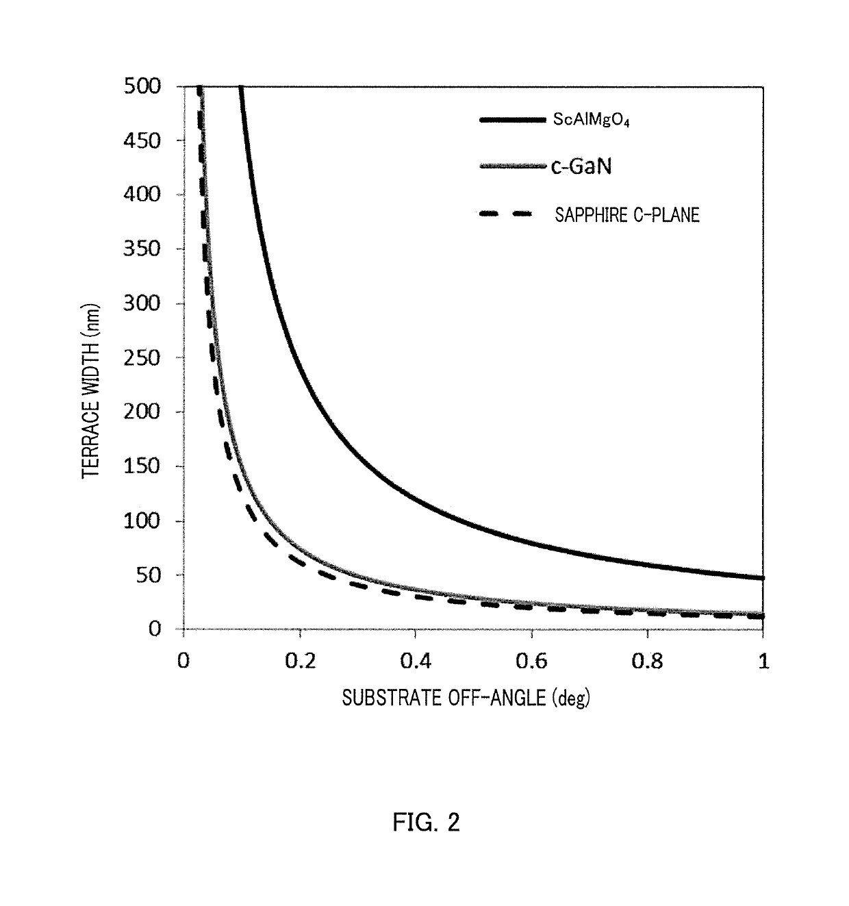
[0028]The crystal structure of ScAlMgO4 is shown in FIG. 1. The crystal of ScAlMgO4 takes a structure in which a MgAlO2 layer as a hexagonal crystal and a ScO layer having a rock salt structure are layered in a [0001] direction (C-axis direction). A (0001) plane (C plane) formed by common cleavage is constituted by a MgAlO2 layer. In the crystal of ScAlMgO4, the crystal lattice constant (c) in the [0001] direction is 25.160 Å, and a step height, which appears by forming an off-angle, will be 25.160 / 3=8.387 Å. This step height is a relatively large value, as compared with the step height (2.593 Å) appearing in a GaN substrate, which is a group III nitride, and the step height (2.165 Å) appearing in a sapphire substrate (C-plane). The step height also influences a length parallel to the (0001) plane of the step (terrace width). As shown in FIG. 2, the ScAlMgO4 crystal, even when allowed to have an off-angle equivalent to that of a GaN substrate or sapphire substrate, will have a surfa...
embodiment 2
[0044]Subsequently, the ScAlMgO4 substrate of Embodiment 2 will be described. In the ScAlMgO4 substrate of the present embodiment, the main plane has an off-angle b (θb) in a direction substantially parallel to the M-plane (1-100) from the C-plane (0001) plane but has no off-angle a, that is, the main plane has an off-angle b tilted θb° with respect to the A-axis direction [11-20] from the C-plane (0001). A method for producing a ScAlMgO4 substrate having such an off-angle b is the same as the method for producing a ScAlMgO4 substrate of Embodiment 1 aforementioned. However, in the aforementioned off-angle formation, the off-direction and the off-angle are adjusted.
[0045]The preferable range of the off-angle b in the ScAlMgO4 substrate of the present embodiment is 0.05°≤|θb|≤0.4°, more preferably 0.1°≤|θb|≤0.4°, still more preferably 0.1°≤|θb|≤0.4°. Hereinbelow, the reason will be described.
[0046]As in Embodiment 1, a group III nitride semiconductor layer (GaN film) was epitaxially ...
embodiment 3
[0047]Subsequently, the ScAlMgO4 substrate of Embodiment 3 will be described. In the ScAlMgO4 substrate of the present embodiment, the main plane is tilted θa° with respect to the M-axis direction and θb° with respect to the A-axis direction, from the C-plane (0001 plane). That is, the substrate includes the compound off-angle of the off-angle a and the off-angle b. A method for producing a ScAlMgO4 substrate having such an off-angle a and an off-angle b is the same as in Embodiment 1 aforementioned. However, in the aforementioned off-angle formation, the off-direction and the off-angle are adjusted.
[0048]In the ScAlMgO4 substrate of the present embodiment, the range of the off-angle a is preferably 0.05°≤|θa|≤0.8°, more preferably 0.2°≤|θa|≤0.6°. The range of the off-angle b is preferably 0.05°≤|θb|≤0.4°, more preferably 0.1°≤|θb|≤0.4°, still more preferably 0.1°≤|θa|<0.4°. Hereinbelow, the reason will be described.
[0049]As in Embodiment 1, group III nitride semiconductor layer (Ga...
PUM
| Property | Measurement | Unit |
|---|---|---|
| off-angle | aaaaa | aaaaa |
| off-angle | aaaaa | aaaaa |
| off-angle | aaaaa | aaaaa |
Abstract
Description
Claims
Application Information
 - R&D
- Intellectual Property
- Life Sciences
- Materials
- Tech Scout
- Unparalleled Data Quality
- Higher Quality Content
- 60% Fewer Hallucinations
Browse by: Latest US Patents, China's latest patents, Technical Efficacy Thesaurus, Application Domain, Technology Topic, Popular Technical Reports.
© 2025 PatSnap. All rights reserved.Legal|Privacy policy|Modern Slavery Act Transparency Statement|Sitemap|About US| Contact US: help@patsnap.com


