Light emitting device, method for manufacturing light emitting device and lighting system having same

a technology manufacturing methods, applied in the direction of semiconductor devices, basic electric elements, electrical equipment, etc., can solve the problems of deterioration of electrical characteristics and optical characteristics of light emitting devices, and achieve the effect of reducing defects due to potential differences and effectively preventing defects

Active Publication Date: 2019-08-06
SUZHOU LEKIN SEMICON CO LTD
View PDF17 Cites 3 Cited by
  • Summary
  • Abstract
  • Description
  • Claims
  • Application Information

AI Technical Summary

Benefits of technology

[0010]According to the embodiment, aluminum nitride is used as the buffer layer, such that the defect due to the potential difference can be effectively prevented.
[0011]In addition, according to the embodiment, a void is further formed on the buffer layer, such that the defect due to the potential difference can be more effectively blocked.
[0012]In addition, according to the embodiment, the pattern part is formed on the substrate, such that the defect due to the potential difference can be effectively reduced.

Problems solved by technology

However, the defect due to the potential incurs because of the difference in lattice constant between the sapphire used as the substrate and gallium nitride (GaN), which causes a problem that electrical characteristics and optical characteristics of the light emitting device are deteriorated.

Method used


Image

  • Light emitting device, method for manufacturing light emitting device and lighting system having same
  • Light emitting device, method for manufacturing light emitting device and lighting system having same
  • Light emitting device, method for manufacturing light emitting device and lighting system having same

Examples


Embodiment Construction

[0019]Hereinafter, the embodiment will be described in detail with reference to the accompanying drawings.

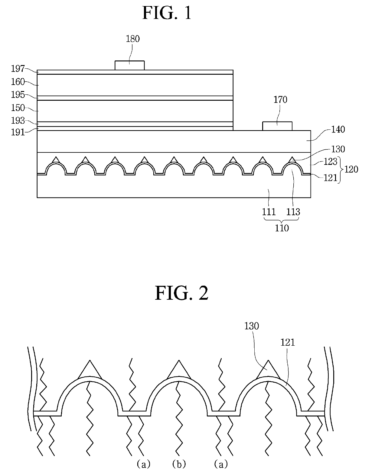
[0020]FIG. 1 is a schematic sectional view illustrating a light emitting device formed therein with a void layer according to an embodiment. FIG. 2 is a schematic sectional view illustrating a state of blocking a potential of a light emitting device formed therein with a void layer according to an embodiment.

[0021]Referring to FIG. 1, the light emitting device according to an embodiment includes a substrate 110, a first buffer layer 121 disposed on the substrate 110, a void layer 130 disposed on the first buffer layer 121, a second buffer layer 123 disposed on the void layer 130, a first conductive semiconductor layer 140 disposed on the second buffer layer 123, a current diffusion layer 191 and a strain control layer 193 disposed on the first conductive semiconductor layer 140, an active layer 150 disposed on the strain control layer 193, an electron blocking layer 195 disposed...


PUM


Abstract

A light emitting device, according to one embodiment, may comprise: a substrate having a pattern part disposed on the upper surface thereof; a first buffer layer disposed on the substrate; a second buffer later disposed on the first buffer layer; a first conductive semiconductor layer disposed on the second buffer layer; an active layer disposed on the first conductive semiconductor layer; a second conductive semiconductor layer disposed on the active layer; and a void layer disposed on the first buffer layer corresponding to the pattern part of the substrate. By further forming a void on the buffer layer, the embodiment has the effect of more effectively preventing defects caused by a potential difference.

Description

CROSS-REFERENCE TO RELATED PATENT APPLICATIONS[0001]This application is a U.S. National Stage Application under 35 U.S.C. § 371 of PCT Application No. PCT / KR2016 / 005671, filed May 27, 2016, which claims priority to Korean Patent Application No. 10-2015-0075845, filed May 29, 2015, whose entire disclosures are hereby incorporated by reference.TECHNICAL FIELD[0002]The embodiment relates to a light emitting device, and more particularly, to a light emitting device for improving light efficiency of the light emitting device, a method for manufacturing the light emitting device and a lighting system having the same.BACKGROUND ART[0003]In general, a light emitting device is a compound semiconductor having a characteristic of converting electrical energy into light energy. The light emitting device may include compound semiconductors belonging to group III and V on the periodic table. The light emitting device can represent various colors by adjusting the composition ratio of the compound ...

Claims


Application Information

Patent Timeline
Patent Type & Authority Patents(United States)
IPC IPC(8): H01L33/20H01L33/12H01L33/58H01L33/42H01L33/22H01L33/00H01L33/06
CPCH01L33/12H01L33/007H01L33/06H01L33/58H01L33/22H01L33/42H01L33/20
Inventor JANG, JUNG HUNNAM, SEUNG KEUNYIM, JEONG SOONCHOI, WON HEE
Owner SUZHOU LEKIN SEMICON CO LTD
Why Eureka
Try Eureka