
Method for producing a solar cell involving doping by ion implantation and depositing an outdiffusion barrier

a solar cell and ion implantation technology, applied in photovoltaic energy generation, electrical equipment, renewable energy products, etc., can solve the problems of reducing the quantum efficiency of the cell, the curing conditions are not ideal for the back surface of the phosphorus, and the practicability of the application, so as to prevent the outdiffusion of phosphorus, slow down the diffusion of phosphorus, and prevent autodoping

Active Publication Date: 2019-04-16
ION BEAM SERVICES
View PDF11 Cites 0 Cited by
  • Summary
  • Abstract
  • Description
  • Claims
  • Application Information

AI Technical Summary

Benefits of technology

This patent describes a method to improve the performance of solar cells by preventing the diffusion of phosphorus during the curing step. By depositing a cap on the rear side of the cell after implantation of the phosphorus and before the curing step, the cap prevents the outdiffusion of phosphorus. This cap can be made impermeable to oxygen to further prevent oxidation-enhanced-diffusion. Additionally, the method includes a process to slow down the diffusion of phosphorus by depositing a layer or layers that inject vacancies into the silicon during the annealing step. This leads to a better performance of the solar cell.

Problems solved by technology

The experiments of the inventors have shown that the practical application was problematic.
These conditions are not ideal for the curing of the phosphorus Back Surface Field (BSF).
This leads to increased Free-Carrier-Absorption which lowers the quantum efficiency of the cell.
This loss of doping agent leads in turn to an increase in contact resistance on the rear side of the cell and may cause short-circuits between emitter and BSF further to a so-called autodoping.

Method used


Image

  • Method for producing a solar cell involving doping by ion implantation and depositing an outdiffusion barrier
  • Method for producing a solar cell involving doping by ion implantation and depositing an outdiffusion barrier
  • Method for producing a solar cell involving doping by ion implantation and depositing an outdiffusion barrier

Examples


Embodiment Construction

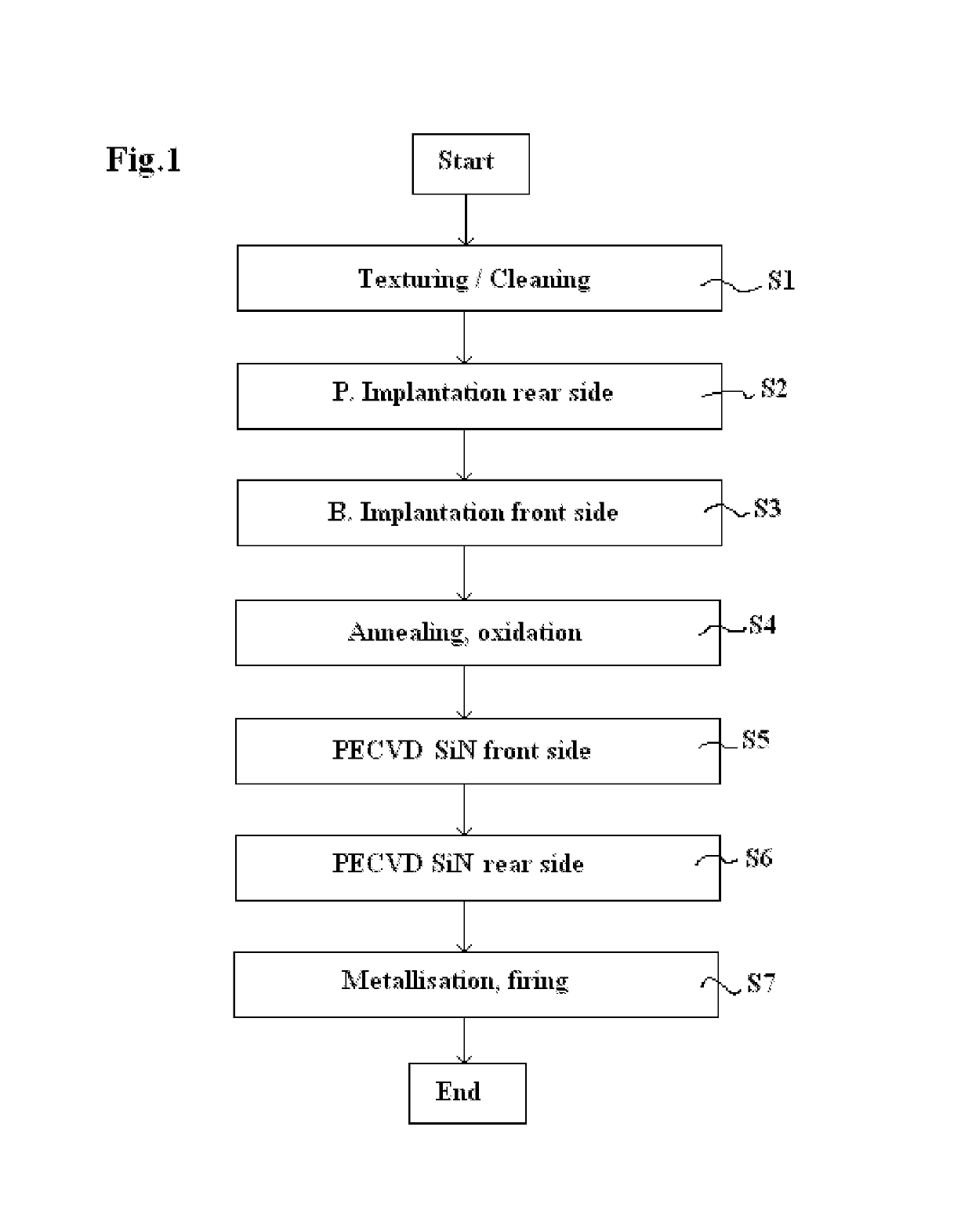
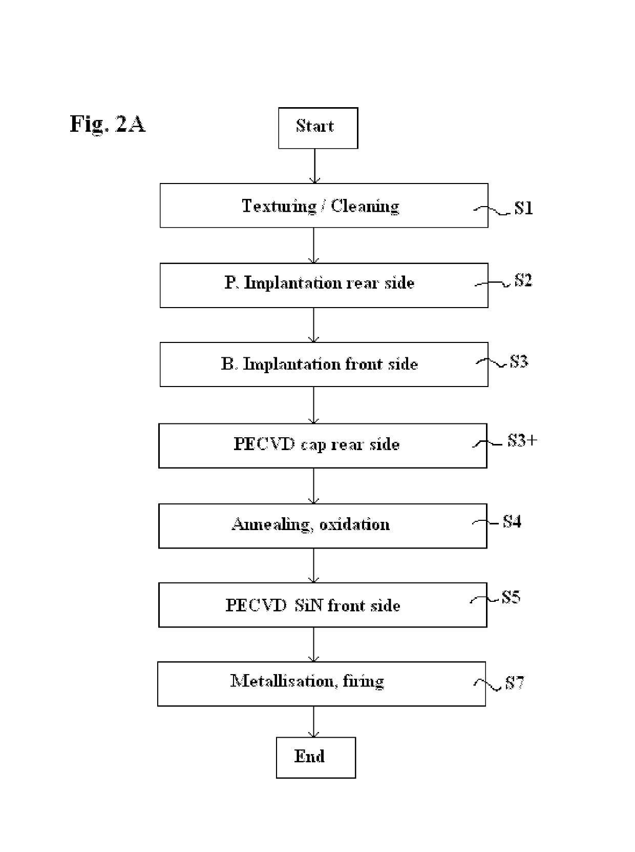
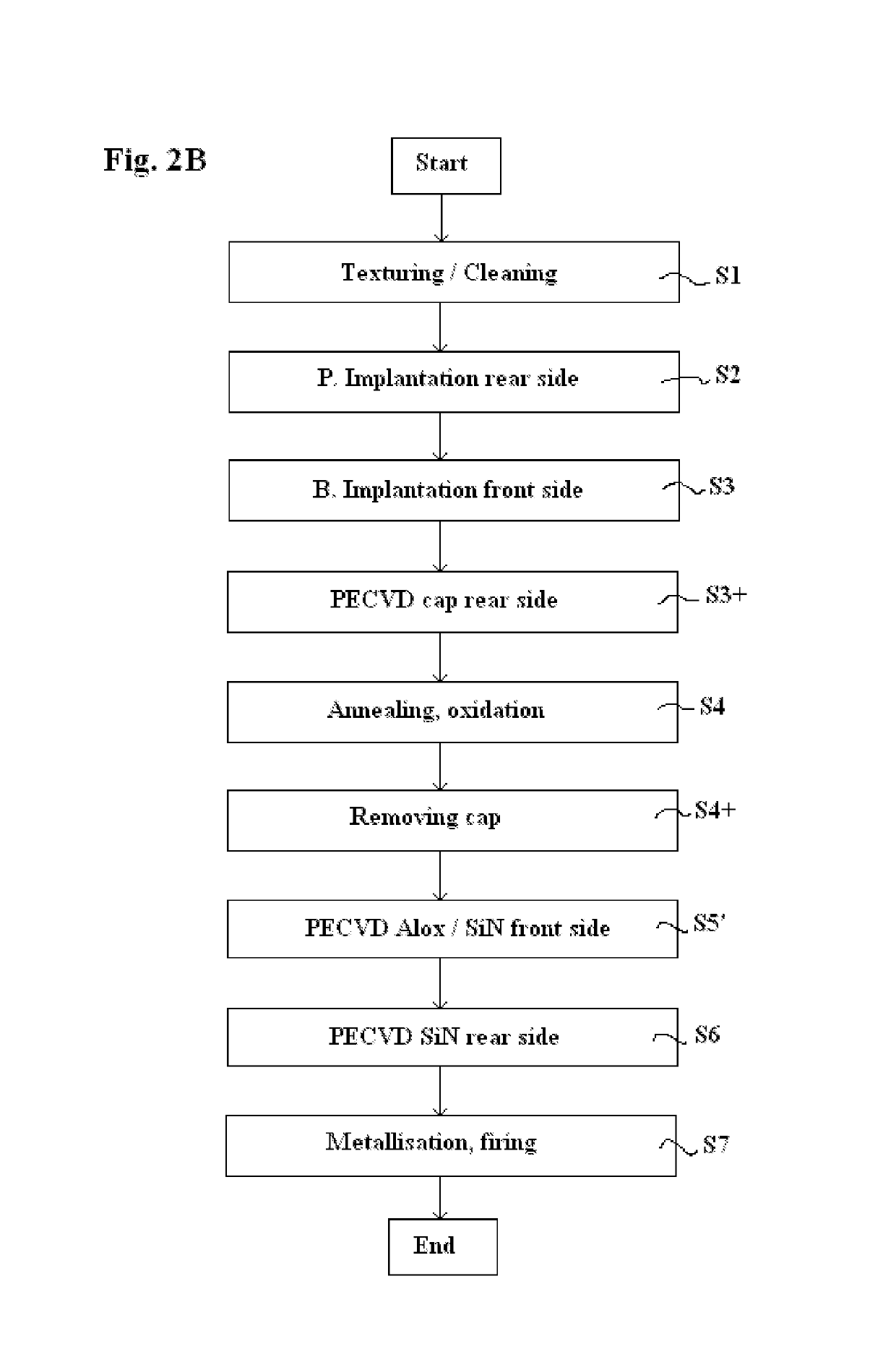
[0022]FIG. 2A shows diagrammatically in a flow chart important steps of the production of a crystalline solar cell in one embodiment of the method according to the invention, whereas the representation is again rather self-explanatory. With respect to the previous process flow shown in FIG. 1, a cap is provided on the rear side of the substrate by means of PECVD (step S3+) after the steps of phosphorus implantation into the rear side of the substrate and of boron implantation into the front side of the substrate (S3), followed in standard sequence by an annealing (step S4) connected to the oxidation of the substrate surface. The cap produced in step S3+ remains as an anti-reflection / passivation layer on the substrate so that the step S6 of the standard process sequence is here dispensed with.

[0023]In contrast thereto the sequence sketched in FIG. 2B sets forth the generation of a cap on the rear side of the substrate in step S3+ which will be removed again after the annealing step S...


PUM


Abstract

The invention relates to a method for producing a solar cell (1) from crystalline semiconductor material, wherein a first doping region (5) is formed by means of ion implantation (S2) of a first dopant in a first surface (3a) of a semiconductor substrate (3), and a second doping region (7) is formed by means of ion implantation (S3) or thermal indiffusion of a second dopant in the second surface (3b) of the semiconductor substrate. After the doping of the second surface, a cap (9b) acting as an outdiffusion barrier for the second dopant is applied and an annealing step (S4) is subsequently carried out.

Description

CROSS REFERENCE TO RELATED APPLICATIONS[0001]This application is a National Stage of International Application No. PCT / EP2014 / 066856, filed on Aug. 5, 2014, which claims priority based on German Patent Application No. 10 2013 218 351.8, filed on Sep. 13, 2013, the contents of all of which are incorporated herein by reference in their entirety.[0002]The invention concerns a method for producing a solar cell from crystalline semiconductor material, wherein in a first surface of a semiconductor substrate a first doping region is formed by ion implantation of a first dopant and in the second surface of the semiconductor substrate a second doping region is formed by ion implantation or thermal indiffusion of a second dopant.STATE OF THE ART[0003]Solar cells based on mono or polycrystalline semiconductor material, in particular silicon, constitute in spite of the development and the launching of the market of new generations of solar cells, such as thin film and organic solar cells, the l...

Claims


Application Information

Patent Timeline
Patent Type & Authority Patents(United States)
IPC IPC(8): H01L31/18H01L31/0216H01L31/068H01L21/265
CPCH01L31/1804H01L21/26513H01L31/02167H01L31/1864H01L31/068Y02P70/521Y02E10/547Y02P70/50H01L31/0288H01L31/0392H01L31/18
Inventor BOESCKE, TIMKANIA, DANIELSCHOELLHORN, CLAUS
Owner ION BEAM SERVICES
Learn More