Optical member and image display device including optical member
an image display device and optical member technology, applied in the direction of instruments, computing, electric digital data processing, etc., can solve the problems of insufficient increase of the intensity of reflected light in the respective direction, difficult to obtain high reflecting properties, etc., and achieve high retroreflection properties
- Summary
- Abstract
- Description
- Claims
- Application Information
AI Technical Summary
Benefits of technology
Problems solved by technology
Method used
Image


Examples
example 1
(Preparation of Underlayer)
[0192]A composition shown below was stirred and dissolved in a container held at 25° C. to prepare an underlayer-forming solution.
Underlayer-Forming Solution (Part(s) by Mass)
[0193]Propylene glycol monomethyl ether acetate: 67.8
[0194]Dipentaerythritol hexaacrylate (trade name: KAYARAD DPHA, manufactured by Nippon Kayaku Co., Ltd.): 5.0
[0195]MEGAFACE RS-90 (manufactured by DIC Corporation): 26.7
[0196]IRGACURE 819 (manufactured by BASF SE): 0.5
[0197]The underlayer-forming solution prepared as described above was applied to a transparent polyethylene terephthalate (PET; COSMOSHINE A4100, manufactured by Toyobo Co., Ltd.) substrate having a thickness of 100 μm using an bar coater in an application amount of 3 mL / m2. Next, the underlayer-forming solution was heated such that the film surface temperature was 90° C., and then was dried for 120 seconds. Next, in a nitrogen purged atmosphere having an oxygen concentration of 100 ppm or lower, 700 mJ / cm2 of ultravio...
examples 2 to 16
[0222]Optical members with the overcoat layer were prepared using the same preparation method as in Example 1, except that the amount of DPHA in the underlayer-forming solution, the amount of the chiral agent in the cholesteric liquid crystal ink solution, the dot diameter during ink jet printing, and whether or not the overcoat layer was provided were changed as shown in the following table.
[0223]
TABLE 1Amount ofChiral AgentDotinDiameterAmount ofCholestericDuringDPHA inLiquidInkOver-Under-Crystal InkJetcoatlayerSurfactantSolutionPrintingLayerExample 15Included3.850FormedExample 215Included3.850FormedExample 30Included3.850FormedExample 415Included3.830FormedExample 50Included3.830FormedExample 615Included3.880FormedExample 75Included3.880FormedExample 80Included3.880FormedExample 915Included3.8120FormedExample 100Included3.8120FormedExample 115Included3.880NotFormedExample 120Included3.850NotFormedExample 130Included3.830NotFormedExample 145Included3.550FormedExample 1515Included4....
example 17
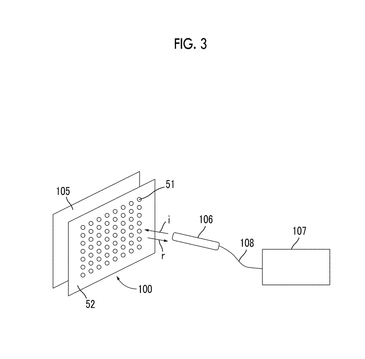
[0225]An optical member with the overcoat layer was prepared using the same preparation method as in Example 1, except that: the addition amount of the chiral agent was changed to 5.8 parts by mass; and the distance between dot centers during ink jet printing was changed to 53 μm. In addition, using an visible and near-infrared light source (HL-2000, manufactured by Ocean Optics Inc.), a ultra high-resolution multi-channel fiber spectrophotometer (HR4000), and a 2-branched optical fiber, the wavelength selective reflecting properties of the optical member with the overcoat layer were measured in 5 arbitrary visual fields having a diameter of 2 mm. In all the visual fields, the reflection peak wavelengths were 550 nm, and all the dots constantly exhibited retroreflection properties in a polar angle range of 0 to 70 degrees and in an azimuthal angle range of 0 to 360 degrees in a case where the normal line perpendicular to the optical member was set as 0 degrees.
PUM
| Property | Measurement | Unit |
|---|---|---|
| angle | aaaaa | aaaaa |
| angle | aaaaa | aaaaa |
| wavelength selective reflecting properties | aaaaa | aaaaa |
Abstract
Description
Claims
Application Information
 - R&D
- Intellectual Property
- Life Sciences
- Materials
- Tech Scout
- Unparalleled Data Quality
- Higher Quality Content
- 60% Fewer Hallucinations
Browse by: Latest US Patents, China's latest patents, Technical Efficacy Thesaurus, Application Domain, Technology Topic, Popular Technical Reports.
© 2025 PatSnap. All rights reserved.Legal|Privacy policy|Modern Slavery Act Transparency Statement|Sitemap|About US| Contact US: help@patsnap.com