
Nanostructured vanadium oxide uncooled bolometers and method of fabrication

Inactive Publication Date: 2019-01-22
NASA
View PDF11 Cites 2 Cited by
  • Summary
  • Abstract
  • Description
  • Claims
  • Application Information

AI Technical Summary

Benefits of technology

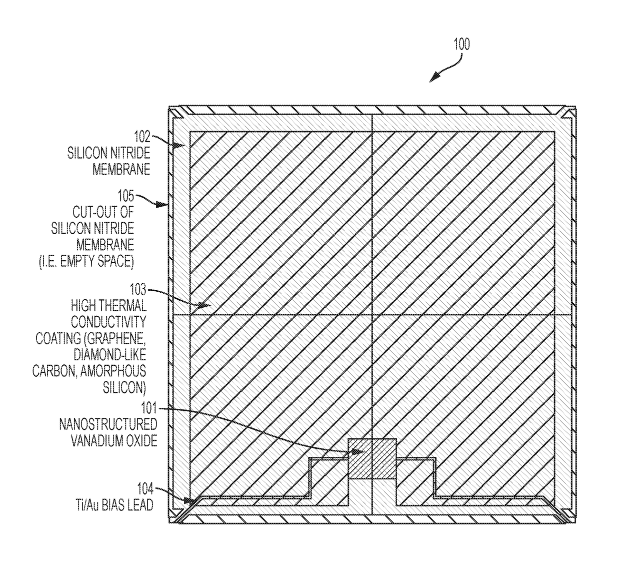
The patent describes a method to improve the heat transfer in a device by adding a layer of thermally conductive material, such as silicon or graphene, to the surface of a nitride or oxide film. This helps to reduce the time it takes to transfer heat within the device.

Problems solved by technology

The detector material, which is thermally well coupled to the absorber is heated, which results in a change of its electrical resistance.
One problem with existing, commercial microbolometers, is that their specific detectivity divided by time constant, D* / t, is too low for applications such as thermal land imaging instruments.

Method used


Image

  • Nanostructured vanadium oxide uncooled bolometers and method of fabrication

Examples


Embodiment Construction

[0023]The present invention relates to a nanostructured, vanadium oxide (VOx) coating which is incorporated as the sensing element of thermal instruments, such as uncooled microbolometers, engaged in applications such as sustainable land imaging by observatories.

[0024]In one exemplary embodiment, uncooled vanadium oxide (VOx) coatings are manufactured as a viable option for thermal imaging instruments, to increase the temperature coefficient of resistance (TCR) of the VOx thermistor. Another exemplary embodiment would entail reducing the internal thermal time constant by depositing a thin, thermally conductive thin film on the membrane containing the VOx like amorphous silicon (Si), graphene, or diamond-like carbon. The TCR of VOx could be increased to a value of 6.5 / K % using ion beam sputtering and post-annealing. Ion beam sputtering is a highly specialized deposition technique, which is available in very few laboratory facilities.

[0025]Thus, the present invention is directed to t...


PUM

PropertyMeasurementUnit
Lengthaaaaaaaaaa
Timeaaaaaaaaaa
Electrical conductoraaaaaaaaaa

Abstract

The present invention relates to uncooled microbolometers which can be integrated in future thermal instruments engaged in land imaging on future observatories. The present invention includes: (1) developing and characterizing a microstructured VOx thin film, and, (2) fabricating an uncooled microbolometer array over the 8-14 micron spectral band.

Description

ORIGIN OF THE INVENTION[0001]The invention described herein was made by an employee of the United States Government, and may be manufactured or used by or for the Government for governmental purposes without the payment of any royalties thereon or therefor.BACKGROUND OF THE INVENTION1. Field of the Invention[0002]The present invention relates to a nanostructured, vanadium oxide (VOx) coating which is incorporated as the sensing element of thermal instruments, such as uncooled microbolometers, engaged in applications such as sustainable land imaging by observatories. The present invention is directed to fabricating the VOx thin film bolometer, including: (1) depositing a vanadium oxide (VOx) thin film on a silicon nitride substrate, and developing and characterizing the microstructured thin film, and (2) fabricating thermal instrument mechanical models, such as an uncooled microbolometer array, over ultrathin silicon nitride membranes (i.e., over the 8-14 micron spectral band).2. Des...

Claims


Application Information

Patent Timeline
IPC IPC(8): G01J5/20C23C14/35C23C14/34C23C14/00C23C14/16C23C14/58C23C14/08
CPCG01J5/20C23C14/083C23C14/5826C23C14/3464C23C14/0036C23C14/165C23C14/35C23C14/5873G01J5/024C23C14/3492
Inventor BROWN, ARI D.BARRENTINE, EMILY M.ASLAM, SHAHID
Owner NASA
Learn More