Mitigating read errors following programming in a multi-level non-volatile memory

a non-volatile memory and read error technology, applied in the field of data processing and data storage, can solve problems such as unacceptable read performance, and achieve the effect of reducing the number of read errors and reducing the number of errors

Active Publication Date: 2018-10-16
IBM CORP
View PDF8 Cites 25 Cited by
  • Summary
  • Abstract
  • Description
  • Claims
  • Application Information

AI Technical Summary

Benefits of technology

[0005]The present disclosure appreciates that there is a waiting period before a recently programmed page in multi-level NAND flash can be read without an increased number of read errors. This period may be dependent on the time required for the programmed threshold voltage distributions to settle to their final state along with any other physical relaxation mechanism that may take place and which may be dependent on the underlying NAND flash technology. Specifically, for MLC NAND flash with a two-step programming process, the waiting period after programming an upper page should be preserved before reading that upper page or its associated lower page. Moreover, the present disclosure appreciates that waiting until the recommended period has elapsed before allowing a recently programmed page of multi-level flash memory to be read can result in unacceptable read performance. The present disclosure accordingly provides one or more techniques that mitigate errors induced by read accesses to recently programmed pages of a non-volatile memory.

Problems solved by technology

Moreover, the present disclosure appreciates that waiting until the recommended period has elapsed before allowing a recently programmed page of multi-level flash memory to be read can result in unacceptable read performance.

Method used


Image

  • Mitigating read errors following programming in a multi-level non-volatile memory
  • Mitigating read errors following programming in a multi-level non-volatile memory
  • Mitigating read errors following programming in a multi-level non-volatile memory

Examples


Embodiment Construction

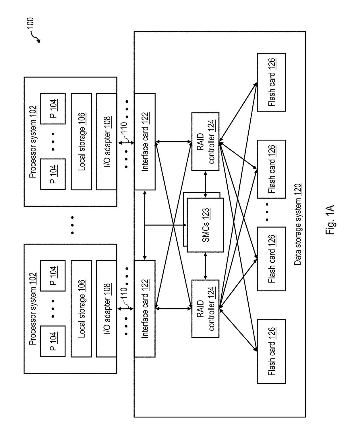
[0016]With reference to the figures and with particular reference to FIG. 1A, there is illustrated a high level block diagram of an exemplary data processing environment 100 including a data storage system 120 having a non-volatile memory array as described further herein. As shown, data processing environment 100 includes one or more hosts, such as a processor system 102 having one or more processors 104 that process instructions and data. A processor system 102 may additionally include local storage 106 (e.g., dynamic random access memory (DRAM) or disks) that may store program code, operands and / or execution results of the processing performed by processor(s) 104. In various embodiments, a processor system 102 can be, for example, a mobile computing device (such as a smartphone or tablet), a laptop or desktop personal computer system, a server computer system (such as one of the POWER series of servers available from International Business Machines Corporation), or a mainframe co...


PUM


Abstract

Read errors following programming in a multi-level non-volatile memory are mitigated by a controller of the non-volatile memory. The controller temporarily buffers, in a cache, pages of data programmed into the non-volatile memory. In response to receiving a read request for a target page of data programmed into the non-volatile memory, where the read request is received during a delay time affecting the target page, the controller services the read request by accessing data of the target page in the cache in response to the read request hitting in the cache. The controller instead services the read request from the non-volatile memory in response to the read request missing in the cache. When servicing the read request from the non-volatile memory, the controller preferably reads the target page from the non-volatile memory utilizing a set of read voltage thresholds determined based on the read-after-write delay.

Description

BACKGROUND OF THE INVENTION[0001]This disclosure relates to data processing and data storage, and more specifically, to non-volatile memory storing multiple bits of data per cell. Still more particularly, the disclosure relates mitigating read errors following programming in a non-volatile memory system storing multiple bits of data per cell.[0002]NAND flash memory is an electrically programmable and erasable non-volatile memory technology that stores one or more bits of data per memory cell as a charge on the floating gate of a transistor or a similar charge trap structure. The amount of charge on the floating gate modulates the threshold voltage of the transistor. By applying a proper read voltage and measuring the amount of current, the programmed threshold voltage of the memory cell can be determined and thus the stored information can be detected. Memories storing one, two, three and four bits per cell are respectively referred to in the art as Single Level Cell (SLC), Multi-Le...

Claims


Application Information

Patent Timeline
Patent Type & Authority Patents(United States)
IPC IPC(8): G11C11/34G06F12/1009G06F3/06
CPCG06F3/0619G06F3/0688G06F3/0659G06F3/0625G06F12/1009G06F2212/65G06F3/0656G06F12/0246G06F12/0866G06F2212/1032G06F2212/214G06F2212/262G06F2212/312G06F2212/7201G06F2212/7206
Inventor CAMP, CHARLES J.FISHER, TIMOTHY J.FRY, AARON D.IOANNOU, NIKOLASMITTELHOLZER, THOMASPAPANDREOU, NIKOLAOSPARNELL, THOMASPLETKA, ROMANPOZIDIS, CHARALAMPOSTOMIC, SASA
Owner IBM CORP
Why Eureka
Try Eureka