Vertical field effect transistor (VFET) having a self-aligned gate/gate extension structure and method

a technology of vertical field effect transistor and gate extension structure, which is applied in the direction of basic electric elements, electrical apparatus, semiconductor devices, etc., can solve the problems of consuming additional chip area, corresponding increase in short channel effects, and risking the formation of defects (e.g., shorts),

Active Publication Date: 2018-09-04
GLOBALFOUNDRIES US INC
View PDF11 Cites 9 Cited by
  • Summary
  • Abstract
  • Description
  • Claims
  • Application Information

AI Technical Summary

Benefits of technology

[0010]For example, one embodiment of the method can include forming one or more vertical field effect transistors (VFETs) on a substrate by forming a fin-shaped body on a substrate such that the fin-shaped body includes a semiconductor fin having first opposing sidewalls and an isolation fin positioned laterally immediately adjacent to and in end-to-end alignment with the semiconductor fin and having second opposing sidewalls. Source/drain regions can be formed, during processing, such that this semiconductor fin extends essentially vertically between a first source/drain region and a second source/drain region. A gate can be formed such that it has both a main section and an extension section. The main section can be adjacent to the first op...

Problems solved by technology

Unfortunately, the smaller channel lengths resulted in a corresponding increase in short channel effects.
As the device density (i.e., the number of devices per unit area) of IC designs continues to be increased, forming the above-mentioned non-planar FETs without ...

Method used


Image

  • Vertical field effect transistor (VFET) having a self-aligned gate/gate extension structure and method
  • Vertical field effect transistor (VFET) having a self-aligned gate/gate extension structure and method
  • Vertical field effect transistor (VFET) having a self-aligned gate/gate extension structure and method

Examples


embodiment 100

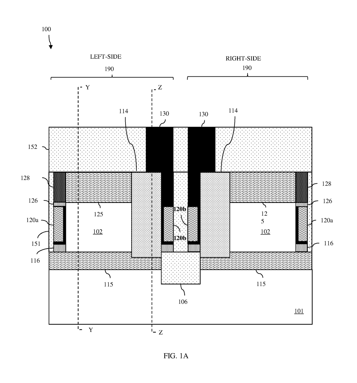
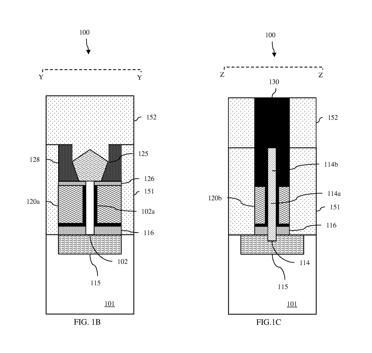
[0053]As illustrated in FIGS. 1A-1C, in the embodiment 100 each VFET 190 can have a discrete fin-shaped body that includes both the semiconductor fin 102 and the isolation fin 114. Specifically, within each discrete fin-shaped body, the semiconductor fin 102 can be above and immediately adjacent to the semiconductor substrate 101 and can have a first outer end and a first inner end opposite the first outer end. Furthermore, within each discrete fin-shaped body, the isolation fin 114 can be above and immediately adjacent to the semiconductor substrate 101 and can have a second inner end, which is positioned laterally immediately adjacent to the first inner end of the semiconductor fin 102, and a second outer end opposite the second inner end. Additionally, an isolation region 106 can be positioned within the semiconductor substrate 101 and can extend laterally between adjacent isolation fins 114 of adjacent fin-shaped bodies. The isolation region 106 can extend deeper into the semico...

embodiment 200

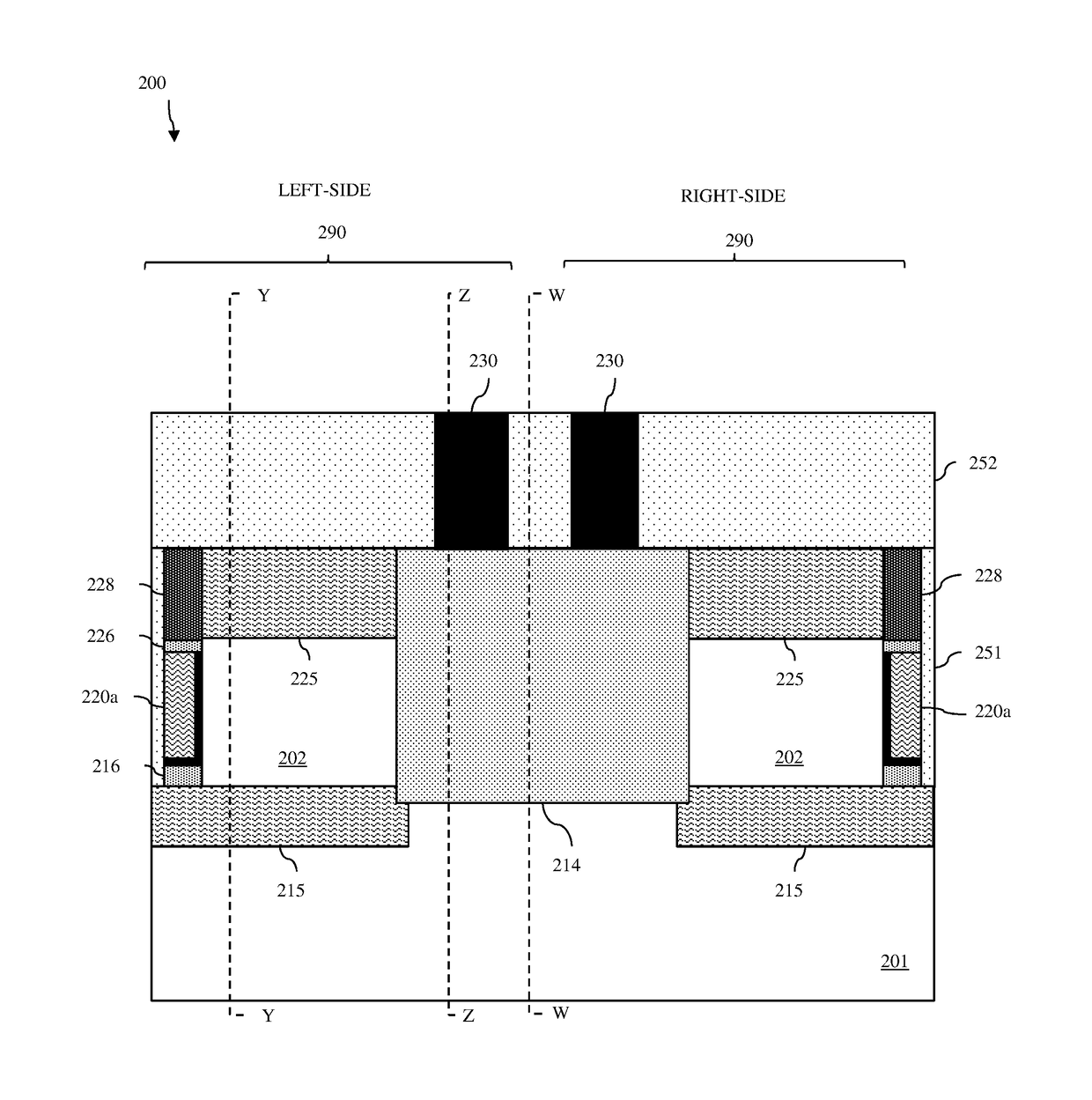
[0054]As illustrated in FIGS. 2A-2D, in the embodiment 200, adjacent VFETs 290 can share a single fin-shaped body, which includes two semiconductor fins 202 (i.e., a semiconductor fin and an additional semiconductor fin) and an isolation fin 214 that is positioned laterally immediately adjacent to, between, and in end-to-end alignment with the two semiconductor fins 202. In this case, each semiconductor fin 202 can be above and immediately adjacent to the semiconductor substrate 201 and can have an outer end and an inner end opposite the outer end. The isolation fin 214 can also be above and immediately adjacent to the semiconductor substrate 201 and can have opposing ends adjacent to the inner ends of the two semiconductor fins 202, respectively. Isolation regions 207 can be positioned within the semiconductor substrate 201 immediately adjacent to the bottom edges of the opposing ends of the isolation fin 214, can extend laterally the full length of the isolation fin 214 from semic...


PUM


Abstract

Disclosed are embodiments of a semiconductor structure that includes a vertical field effect transistor (VFET). The VFET has a fin-shaped body that includes a semiconductor fin and an isolation fin. The semiconductor fin extends vertically between lower and upper source/drain regions. The isolation fin is adjacent to and in end-to-end alignment with the semiconductor fin. The VFET gate has a main section that wraps around an outer end and opposing sidewalls of the semiconductor fin and an extension section that extends from the main section along at least the opposing sidewalls of a lower portion the isolation fin and, optionally, around an outer end of that lower portion. A gate contact lands on the isolation fin and extends along the opposing sidewalls and, optionally, the outer end of the isolation fin down to the extension section. Also disclosed are method embodiments for forming these structures.

Description

BACKGROUNDField of the Invention[0001]The present invention relates to vertical field effect transistors (VFETs) and, more particularly, a VFET with a combined gate / gate extension structure that is self-aligned and a method of forming the VFET.Description of Related Art[0002]Integrated circuit (IC) design decisions are often driven by device scalability, device density, manufacturing efficiency and costs. For example, size scaling of planar field effect transistors (FETs) resulted in the development of planar FETs with relatively short channel lengths. Unfortunately, the smaller channel lengths resulted in a corresponding increase in short channel effects. In response, non-planar FET technologies have been developed.[0003]Exemplary non-planar technologies include, for example, standard fin-type FETs (FINFETs) and vertical fin-type FETs (VFETs). A FINFET is a non-planar FET that incorporates a semiconductor fin (i.e., a relatively tall and thin, initial, rectangular-shaped, semicondu...

Claims


Application Information

Patent Timeline
IPC IPC(8): H01L29/78H01L29/66H01L21/768H01L29/423H01L21/8234
CPCH01L29/66545H01L29/7827H01L21/76897H01L29/42376H01L21/823481H01L21/823487
Inventor ZANG, HUI
Owner GLOBALFOUNDRIES US INC
Why Eureka
Try Eureka