Polymer light-emitting-diode making method

A technology of light-emitting diodes and manufacturing methods, which is applied in semiconductor/solid-state device manufacturing, electrical components, electric solid-state devices, etc., can solve the problems of low luminous purity of polymer light-emitting diodes, and achieve the effect of improving luminous purity

Inactive Publication Date: 2007-06-13
INNOCOM TECH SHENZHEN +1
View PDF0 Cites 0 Cited by
  • Summary
  • Abstract
  • Description
  • Claims
  • Application Information

AI Technical Summary

Problems solved by technology

[0008] In order to solve the problem of low luminous purity of the polymer light-emitting diodes obtained by the prior art polymer light-emitting diode manufacturing method, it is necessary to provide a polymer light-emitting diode manufacturing method that can manufacture polymer light-emitting diodes with higher luminous purity

Method used


Image

  • Polymer light-emitting-diode making method

Examples


Embodiment Construction

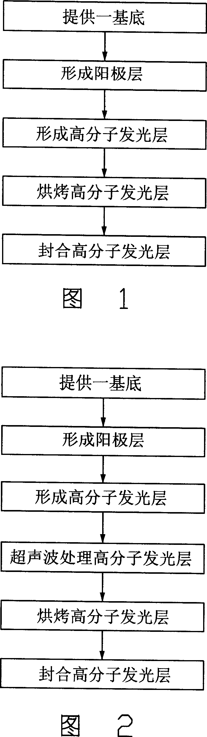
[0013] Please refer to FIG. 2 , which is a flow chart of a preferred embodiment of the manufacturing method of the polymer light emitting diode of the present invention. The manufacturing method of the polymer light-emitting diode comprises the following steps: providing a base; forming an anode layer on the base; forming a polymer light-emitting layer on the anode layer; ultrasonically treating the polymer light-emitting layer; baking the polymer light-emitting layer ; Sealing the polymer light-emitting layer. details as follows:

[0014] (1) Provide a base

[0015] The substrate acts as a carrier for other components, and its material is usually glass, organic film or plastic.

[0016] (2) Forming the anode layer

[0017] The anode layer is formed on the substrate. The anode layer may be a transparent conductive material, such as indium tin oxide (ITO) or indium zinc oxide (IZO), or a thin metal conductive film through which light can pass. The anode layer can be formed...


PUM


Abstract

The method for fabricating high molecular light emitting diode (LED) includes steps: providing a base plate; forming an anode layer on the base plate; forming a high molecular luminous layer on the anode layer; using ultrasonic to process the high molecular luminous layer. The method can produce high molecular LED with higher purity of luminescence.

Description

【Technical field】 [0001] The invention relates to a method for manufacturing a polymer light-emitting diode. 【Background technique】 [0002] With the rapid development of science and technology, people's requirements for display devices are also increasing day by day, making the display devices develop in a direction of being lighter, thinner, and more power-saving, and thus organic light-emitting diode displays are produced. Compared with liquid crystal displays, organic light-emitting diode displays are self-illuminating displays, and do not require a backlight module with high energy consumption, so they can be lighter, thinner, and more power-saving. [0003] According to the different organic thin film materials used, organic light emitting diodes can be divided into small molecule light emitting diodes and polymer light emitting diodes. [0004] Organic light-emitting diodes usually include a multi-layer film structure such as an electron injection layer, an electron ...

Claims


Application Information

Patent Timeline
Patent Type & Authority Applications(China)
IPC IPC(8): H01L51/56
Inventor 黄荣龙彭家鹏
Owner INNOCOM TECH SHENZHEN
Why Eureka
Try Eureka